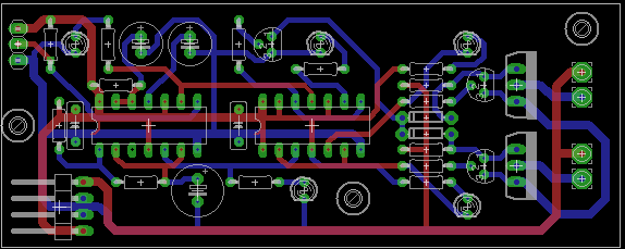
I’m working on a PC board layout for a circuit I’ve built and tested on the workbench. I enjoy board layout, but I was still delighted to be finished with the design. I printed out a copy, not to test whether all the components fit, but to stare at for a day and see whether I found anything that might need to be corrected.
Boy, did I.
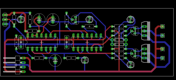
In general, the first stage of laying out a PCB is placing external interface components — connectors, switches, potentiometers, etc. — followed closely by other large components and power supply traces. For me, the last stage of layout is doing a sanity check that the board will actually work (and be possible to assemble) in the real world.
Here’s what I found.
- Since I’m making a single copy of this and never expect to make more, I’m not bothering to have the board produced commercially, but rather having it milled. Milled boards don’t have plated through-holes and vias, so make sure any components whose footprints cover their leads have only bottom-side traces or I won’t be able to solder them. I always keep this in mind during design and I did okay on the LEDs and transistors but I forgot two electrolytic capacitors, the three-pin header in the upper left, and the yet-to-be-determined connectors at the right.
- I find that without plated through holes I need larger solder pads. As a very last step, use the DRC Restring parameters to increase all solder pad sizes. I was already careful to avoid routing traces between IC pins — which I would cheerfully do on a commercially-produced board — knowing that I’d want to increase pad sizes.
- Although this isn’t a high-power project, the traces to the output pins look a little narrow to me, and there’s no reason the other traces shouldn’t be wider as well. I already used wider traces than I do on very small boards, but increase the trace widths even more.
- This PCB is going to get screwed down to a piece of plywood, but I forgot to include mounting holes, or even room for them.
- Yes, yes, double-check that resistors and electrolytic capacitors are drawn at the right size.
- The upper left connector includes ground and 5V for a secondary board, so plugging it in backwards would be catastrophic. The connector should be polarized at a minimum and latching if possible; make sure the footprint still matches the chosen connector type.
- I hadn’t yet decided on output connectors and had just drawn pads to represent them. Choose output connectors and update the footprints accordingly.
- I’ve found that BJTs from different manufacturers — even with the same part number — may have different pinouts; and I’m planning to use no-name BJTs from the scrap bin, so there’s no telling whether their pinouts correspond to what EAGLE thinks. Check the BJT pinouts and adjust accordingly.
- The milled PC board won’t have a silkscreen layer and I may not bother to iron-on the silkscreen layer. Indicate the IC orientation in the top copper layer.
This afternoon I addressed these issues, starting with the ones most likely to require rerouting traces.
Move Electrolytic Capacitor Traces to the Bottom
The two electrolytics in the upper left have top-side traces that would be very hard to solder without leaving the capacitors raised higher above the board than I prefer.
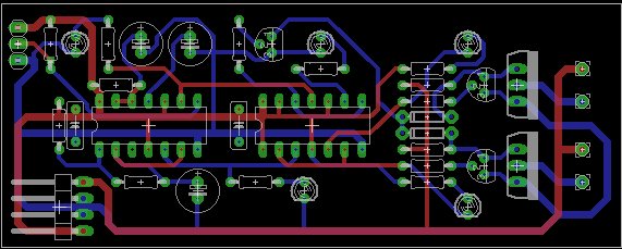
Not too much work to reroute a few traces.
For the input and output connectors, even though the plastic form blocks the top-side solder pads, I leave the top-side traces as they are. I’ve got into the habit of pushing connector pins through their plastic form in order to solder top-side, then pushing the plastic form back down (almost) to the PCB after soldering. I am (over)confident of finding a latching three-pin connector with .1″ spacing that I can solder top-side and I know I can use that trick with the output connectors I have in mind.
Component Sizes
The resistors are the right size, but the capacitor I’ll install in the lower left probably has 3.5mm pin spacing and 8mm diameter rather than 2.5/7. Happily, the updated package doesn’t require repositioning anything else, just bending a trace.

Output Connectors
I have some .156″ bump-latching connectors on hand with .045″-diameter pins. That information allows me to position the output pins and correct their size.
I use the Info tool to display the pad positions and change each to be .022″ closer to its mate (half the difference between .2″ and .156″). I also increase the pads to 3.17mm (.125″) and the holes to 1.1mm (.043″). If the pins fit too tightly, I can drill out the holes slightly without losing much copper.
Mounting Holes
If I were going to produce more than one of this board, I’d go to the effort of repositioning components to leave room for regularly-spaced mounting holes in the corners. But for a single-copy, single-use board, even a couple of holes across from each other should suffice.
Some small-but-adequate wood screws I have on hand have a shaft diameter of .105″ and a head diameter of .210″.
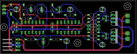
EAGLE has mounting holes available both as components (so you can connect them to a signal, presumably [one of your] ground[s]) and as a tool in the board editor.
Since I don’t particularly care about grounding the board to the plywood enclosure and EAGLE doesn’t have any mounting hole components quite the size I want, I just use the hole tool in the board editor — which means I’m responsible for drawing the screw head clearance myself. I add .15″-radius circles in the tDocu layer around each mounting hole, which should leave clearance for screw heads even slightly larger than what I have on hand.
This necessitates rerouting the power traces at the left edge of the board.
Transistor Pinout
Okay, it’s probably time to talk about the BJTs, but I’ve only been putting it off because I already checked them and I know the answer.
The 2N3904s in EAGLE are CBE when viewed from the front. The unidentified NPNs with which I breadboarded the circuit are EBC.
I wouldn’t do this if I were building more than one, I wouldn’t do this if I were going to have a silkscreen layer, and I wouldn’t do this if anyone other than me or a very close friend were going to assemble the board … but I’m going to leave the layout as-is and install the transistors rotated 180° from what the silkscreen indicates.
IC Orientation
On a milled circuit board on which I may not iron on the silkscreen layer, I like to draw an arc in the top copper layer under the notched end of each IC.

Although it looks odd, it doesn’t matter that the arcs intersect top-side traces as long as they don’t bridge two different traces together.
Trace Widths
I had drawn the board with 40-mil traces for power connections and 24-mil traces for signal connections. On paper, that looks narrow, so I increase it to 50-mil power and 32-mil signal widths.
I use EAGLE’s Change / Width tool to increase the power traces. It seems like there should be a way in the DRC to restring all the remaining traces to a new minimum width, but I don’t find it, so I change them all by hand. In the process, I find that after having moved a component several times, I had a long trace from the left where a short trace from the top would work even better, and I make the correction.
The traces still look narrow on paper, but better.
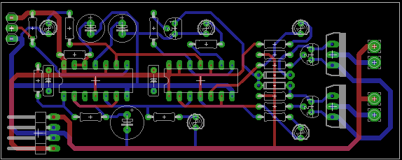
Pad Sizes
All that’s left are pad sizes, which I can do in DRC / Restring.

The default is a copper annulus whose track width (difference between OD and ID) is 25% of the hole diameter (or 50% of the hole radius) and not less than 10 mil. Increasing the minimum to 20 mil gives me lovely, large, solderable pads, but crowds the BJT terminals a bit much for my liking.
Restring operations aren’t undoable, so I reload the copy I saved before the restring (Infocom text adventure, anyone?) and try again. 15 mil looks pretty good and 16 mil looks even better, so I leave it at that — and I barely remember to update the bottom layer minimum as well.
Final Board
After updating the pad sizes, I decide to tweak the top-size power trace just a smidge further away from the left mounting screw head, and then I’m done.
From initial faux-complete:
to real-world updates:
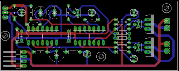
doesn’t look dramatic, but will make a significant difference in ease of assembly. Now it’s ready to mill.
Don’t forget your Z-axis! On a project I did recently, I was going to use board mounted potentiometers. These board mounted pots had a metal sleeve with a washer and nut. I figured I could mount the pots to the panel with the washer and the nut, and the pots are already soldered to the board, so I don’t need any mounting hardware, right?
Then I got my prototype boards back. Turns out I forgot to take into account the height of the capacitors, and I couldn’t mount those pots to anything but the thinnest of metal. Also I wired one of the pots backwards, and since it was a board mounted pot it wasn’t so easy to fix.
Had to switch to external mount pots.
Great article!! I didn’t know about the DRC restring… my latest DIY board suffered from tiny pad syndrome. PITA to solder. Anyway great tips.
I find it’s good to do enough board design to get into a rhythm of design and validation like you.
With recent boards, I start selecting components so I can
pick correct packages in the layout either before doing layout or while.
Also, I got sick of leafing through the eleventy billion different connectors so I now standardize on .1″ pin headers, stock up on vertical and right angle, as well as 2-6 pin female sockets, and call it good.
I’ve forgotten holes on a number of boards I now try to stick those on early.
I usually do a first pass layout, then work on shrinking the footprint from there. Anyway thanks for all the great tips!
Hi Keith.
Interesting article.
One change I would make to your final layout would be to rotate 180 degrees anti-clockwise your two electrolytic caps in the top left hand corner to produce a simple trace layout.
Cheers,
Ross
Ross, it would make for simpler traces, but I’m a believer in consistent orientation of polarized components when possible and I like to put the positive terminals on top. In this design, the wasted traces were worth it to me. Of course, clear, unequivocal labeling is even more important.