Over the weekend I was working on a bidirectional PWM motor speed control circuit with the LogoChip, and I ended up using a 74LS138 demultiplexer to route the PWM signal to the appropriate H-bridge input. (It’s what I had on hand.) Because I wasn’t that familiar with the ’138, I wanted to test it carefully before connecting it to the motor driver. I needed a logic probe, and I didn’t have one.
A logic probe is a tester–usually a small, handheld tester–with a probe that you poke into different parts of your circuit. When you touch a logic connection, the probe lights up an LED to indicate whether the connection is at a high or low logic level. Radio Shack used to sell one for about $30, although I think they’ve discontinued it and I can’t find it in their catalog any more.
In principle, it sounds simple–something that could be built with two TTL buffer gates, one inverting and one non. In practice, there’s a snag that has to do with the definition of TTL logic voltages: a voltage below .5 – .8V is considered a low signal, a voltage above 2.0 – 2.7V is considered a high signal, and a voltage in between is undefined. (Output voltage specifications are stricter and input voltage specs more generous, to account for lossy transmission.)
The obvious implementation–feeding the input into a TTL buffer–would always indicate either high or low, because the buffer will always produce a valid output even if the input is in the “dead zone.” But the probe needs to have both LEDs off when it’s not touching anything or touching something that’s not a high or low logic signal (like a tristated connection, something that isn’t digital logic at all, an output that’s broken, two outputs mistakenly wired together, etc.). Ironically, to indicate the state of a digital signal correctly, you have to use analog electronics.
I’ve wanted a logic probe for years, and although at $30 I could certainly afford one, I never felt it was quite worth buying one. After building my own, I’d have to concur with my previous opinion. ![]()
Different Designs
I searched online and found several logic probe designs, but wasn’t satisfied with any of them. My dissatisfaction fell into two categories:
- Several of the circuits reported whether the input voltage was above or below 2.5V. That’s doubly wrong: they never go dark to indicate absence of a valid signal; and if you’re going to make that mistake, make it around 1.6V, the middle of the “dead zone.”
- Other circuits purported to remain dark when the input was in the TTL dead band, but their schematics were beyond my ability to confirm correct operation. They did things like play tricks with pull-up and pull-down resistors between the probe input and TTL inverter inputs, presumably to try to pull dead-band voltages out of the input range of the buffer. I just wasn’t comfortable with this.
So I designed my own around an LM339 quad comparator chip and some resistors, all from my parts bin.
The Circuit
The key to understanding the circuit is to understand the operation of the LM339. A comparator is an op-amp designed to be used open-loop, to indicate which of two input voltages is higher than the other. The inverting input (labelled -) is subtracted from the non-inverting input (labelled +), and if the resulting voltage is positive, the comparator’s output is high; if the resulting voltage is negative, the comparator’s output is low. That is, if the signal provided to the + input is larger than the one provided to the – input, it indicates high; if the signal provided to the – input is larger, it indicates low. In effect, it compares the two voltages.
Then keep in mind a small trick: Most transistor and IC outputs can sink more current than they source, so I wanted to wire the indicator LEDs from +5V to the comparator output, rather than from the comparator to ground. That means I had to use inverted logic on the outputs, which is accomplished by swapping the inputs. It’s easily done; it just messes with the brain a bit.
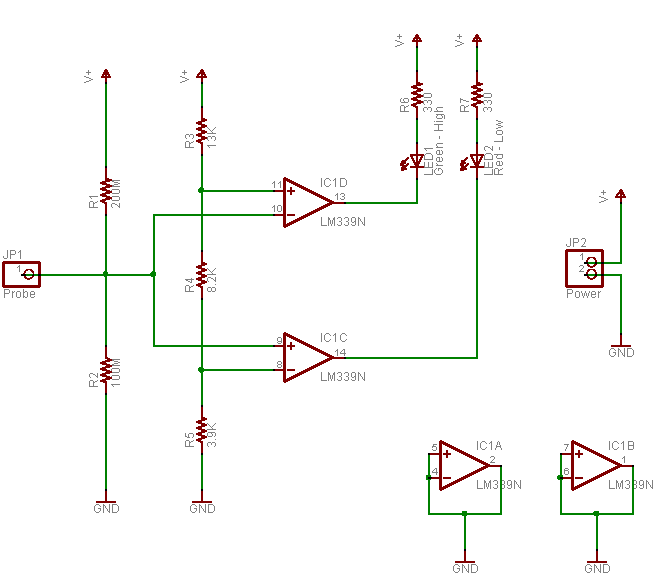
Going through the schematic from left to right, the signal under test is received at the probe input. It’s attached to a high-impedance voltage divider to bias the circuit into the TTL dead band (1.67V) when the probe isn’t touching anything or is touching a high-impedance connection, but which is easily overridden (the bias current is only a few microamps) when a real signal is present.
I built a voltage divider to provide the reference voltages for the TTL low and high voltage levels. I was aiming for .8V and 2.4V; common resistor values of 3.9kΩ, 8.2kΩ, and 13kΩ gave me actual voltages of .78V and 2.41V. Close enough for jazz.
Looking first at the logic-low indicator (which is the lower section on the schematic), the input signal feeds to the non-inverting (+) input of the comparator, with the low reference voltage (.8V from the divider) feeding the inverting input. That means the reference voltage is subtracted from the input voltage, so when the input signal is higher than .8V, the comparator output is high–which leaves the red LED off. (Inverted outputs, remember?) When the input is lower than .8V, the comparator output is low, and the red LED lights.
In contrast, in the logic-high section of the circuit (the upper part of the schematic), the input signal feeds the inverting input of the comparator and the high reference voltage (2.4V) feeds its inverting input. Here the input is subtracted from the reference voltage, so when the input signal is higher than 2.4V, the comparator output is low, lighting the green LED. When the input is lower than 2.4V, the comparator output is high, and the green LED stays off.
The rest of the schematic is housekeeping. Because the LM339 runs as an “infinite-gain” amplifier in an open-loop configuration, it’s subject to self-oscillation, and the datasheet recommends wiring all unused inputs and outputs to ground. And the probe takes its power (and reference VCC) from the circuit under test, so it needs wires to connect to +5V and ground–the jumper at the far right.
Success!
It works like a charm! Because of the inverted logic on the LED-driving outputs, I confused myself about the placements of the inputs a couple of times. But after straightening that out, I haven’t had any problems. It correctly identifies logic levels (and un-identifies non-logic signals), and proved invaluable while troubleshooting my 74LS138 PWM circuit (which will be the subject of another post).
Right now, the probe is built into the rightmost end of the breadboard with my LogoChip, 74LS138, and 74LS04. I’m planning to drill and etch a few dedicated PCBs to make logic probes for myself and some friends, and I’ve just learned to use the Eagle circuit design software–which runs on Mac OS X (among others–another ‘nother post?). W00T!
What’s Missing?
Commerical logic probes have two things that mine doesn’t (not counting a fancy case and a higher price tag): audible output and pulse stretching.
Audible output
Audible output is just what it, er, sounds like: high/low tones played through a little speaker (in conjunction with the LEDs), to indicate high/low logic signals. I don’t think it’d be a big gain for me, but a friend who has one says it’s really handy to be able to focus on keeping the probe tip from slipping off the pin you’re measuring and not have to glance over at the LEDs to check the logic level. I may add that in a future version, or swap probes with him long enough to find out how much it matters to me.
Pulse Stretching
Pulse stretching has to do with the handling of very short pulses. A single bump from low to high of 1ms duration will be detected by the probe and send appropriate current through the high LED, but it’ll probably be so short it can’t be detected (or registered) by the human eye. Pulse-stretching circuitry adds a short-duration timer (say 1/4 second) to the high and low indicators, so that every time a high signal is detected, the indicator lights (and/or sounds) for at least a minimum amount of time (e.g. 1/4 second)–and then for as long as the signal remains at that level. It just gives your eye longer to detect very rapid pulses.
I’m undecided on the topic for my own use, though. I know it’d be annoying to have short pulses coming through and miss them because they were too brief to see. On the other hand, since a lot of what I’m interested in testing right now is PWM signals, I don’t want pulses stretched. PWM is all about repeating rapid pulses, and I prefer to have variable (perceived) LED brightness as an indicator of PWM duty cycle.
I suppose the right answer is to add a switch to select the behavior. Pulse stretching isn’t difficult–it’s just a couple of monostable multivibrators, and the LM339 datasheet shows how I could build them from the two unused gates on the chip I’m already using. That dashes my hopes of dropping from a 14-pin quad comparator to an 8-pin dual comparator and making my logic probe extra slimmy; but sometimes that’s the price you have to pay for greatness.
Voltage Supply
One last consideration is that my circuit “trusts” the voltage supply from the circuit under measurement. The logic probes that I’ve seen all take their power from the test circuit–but mine also divides the circuit’s voltage to get its reference voltages. That means that if the test circuit’s voltage is nonstandard or faulty, my probe will behave differently than expected. It’s unlikely to be damaged–the LM339 can run on a supply voltage of 3-18V–but it wouldn’t necessarily deliver accurate results.
And there’s not much I can do about it without getting a lot fancier–a 7805 regulator needs something like 2.5V of headroom to maintain regulation, and even the more efficient regulators need some headroom. So when the probe is receiving the expected 5V supply, adding a regulator would potentially make it behave worse. I could do something clever stacking diodes to construct a reference voltage, but I’m not sure it’s worth it to me. Guess I might play with it for V2.
I built a logic probe similar but not exactly the same as yours, with plans from another site. Anyways what they did to deal with frequency signals was instead of how you used two separate LED’s they used a bi-color red/green LED. (or a red and green led wired in reverse parallel), anyways I believe if you used A bi-color LED in your circuit A signal You could have three separate outputs. Red = High, Green = Low, Orange = Frequency(sinusoidal, red green red green red green etc)
It would be great if you could find a 1.6v regulator, then you wouldn’t be so dependent on the source voltage being 5v.
Hey,
An electronics tutorial website that I frequent had a logic indicator built from a CMOS inverter, some resistors and some leds. I guess the circuit would not indicate a low level accurately, and a low level would include the “dead zone”. Would there be any way to combine the two designs to include multiple logic probes in one, or add a new feature using the CMOS, or TTL, inverter and your schematic? I was thinking about maybe chaining two inverters together for a low level.
The design is at: http://www.play-hookey.com/digital/experiments/logic_indicators.html.
how would you light up an LED if the voltage is between 0.8 and 2.4?
Sam, that’s not super-easy to do with the LM339 comparator because of the open-collector outputs. What constraints do you have on your question? (For example, one answer is, “Buy a window comparator IC.”)
Hi, Keith, Thanks for the circuit! It appears that Pin #3/VCC has been omitted in the schematic(?) That might be a problem, for a novice. I am an Eagle user, but I have been playing with Fritzing, for this project. I would be glad to give you the files, if you would send me a pm with your email address.