After the 2006 Technology: Art and Sound by Design final exhibit, Steve Atwood worked on building his own LogoBoard to use in his sculpture. He found that his board wasn’t working and was overheating, and asked for my help troubleshooting it. To my recurring shame, I’ve had his board ever since with very little progress to show for it. Time to rectify that.
The Board, the Symptoms, and Initial Efforts
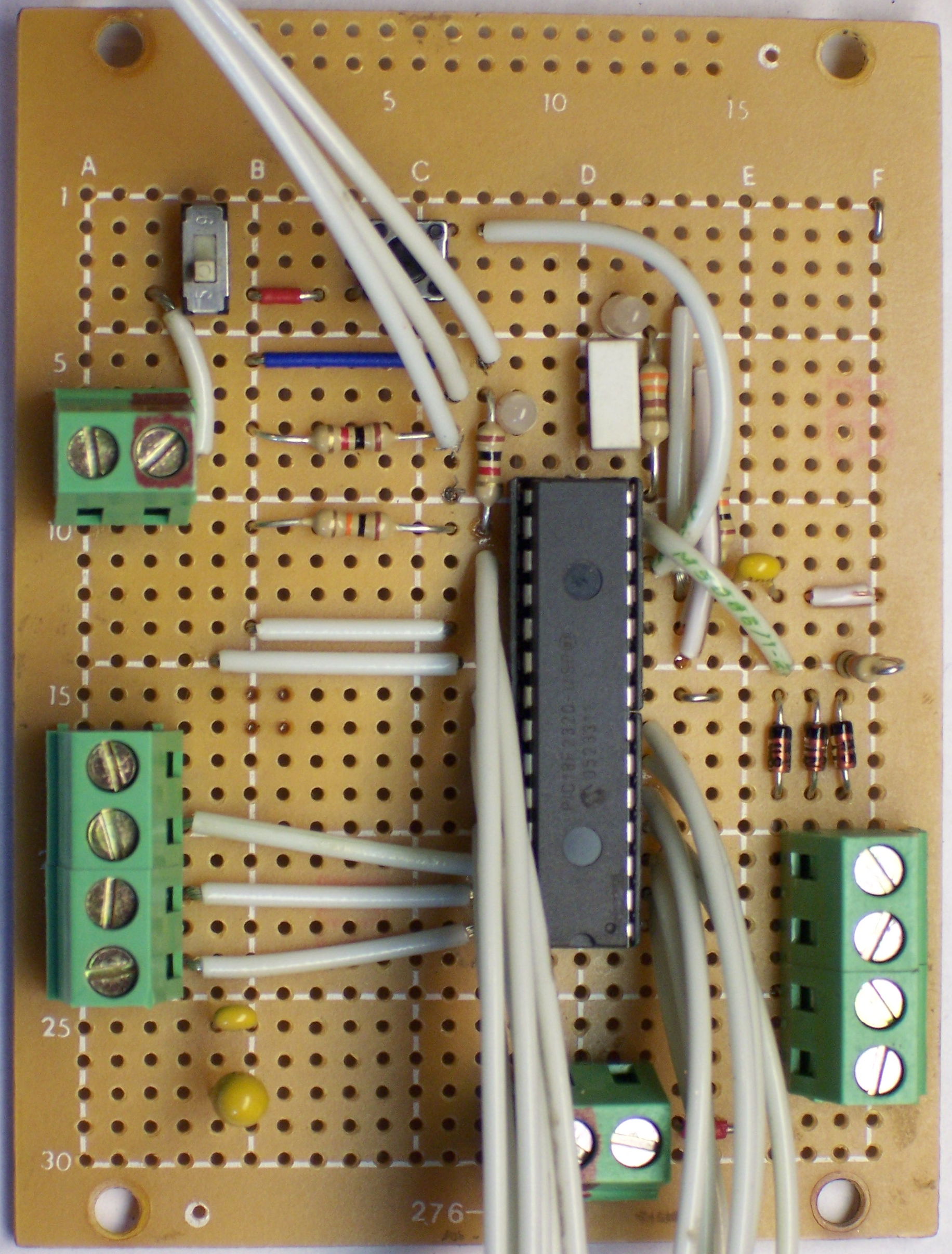
Steve built his circuit on a prototyping board with a .1″ perforated .1″ grid and connecting traces on the back, much like a solderless breadboard. The PIC microcontroller is in the center, with various components, connections, and wires surrounding it.
The main thing I knew when Steve gave me the board was that the LogoChip was overheating. I measured the resistance from the LogoChip’s power pin to ground pin and got some very low value like 4Ω, so I knew something was broken, but not dead shorted. I replaced his chip with one of my own and tested again; mine overheated and had the same resistance as well, so his problem wasn’t just that his chip had burned out.
And there it sat for a year.
Drawing the Schematic
In order to do any further debugging, I needed to determine and draw out exactly what was connected where, so I could examine the schematic and find what looked amiss. And the easiest way I’ve found to make a schematic from a PC board is to recreate the circuit in design software, building out the schematic and a reproduction drawing of the physical PC board at the same time. When the traces on the board drawing match the traces on the board, the schematic is correct and complete.
Working with two windows in EAGLE, I created a new project and added all of the components from Steve’s board. I had to fudge on the screw terminals and the crystal oscillator because I didn’t have library parts for them; but for a quick job like this I feel okay substituting a .1″ header and simply remembering what’s really going on. I carefully placed each component on the PCB diagram at the exact space corresponding to its placement on the real board.
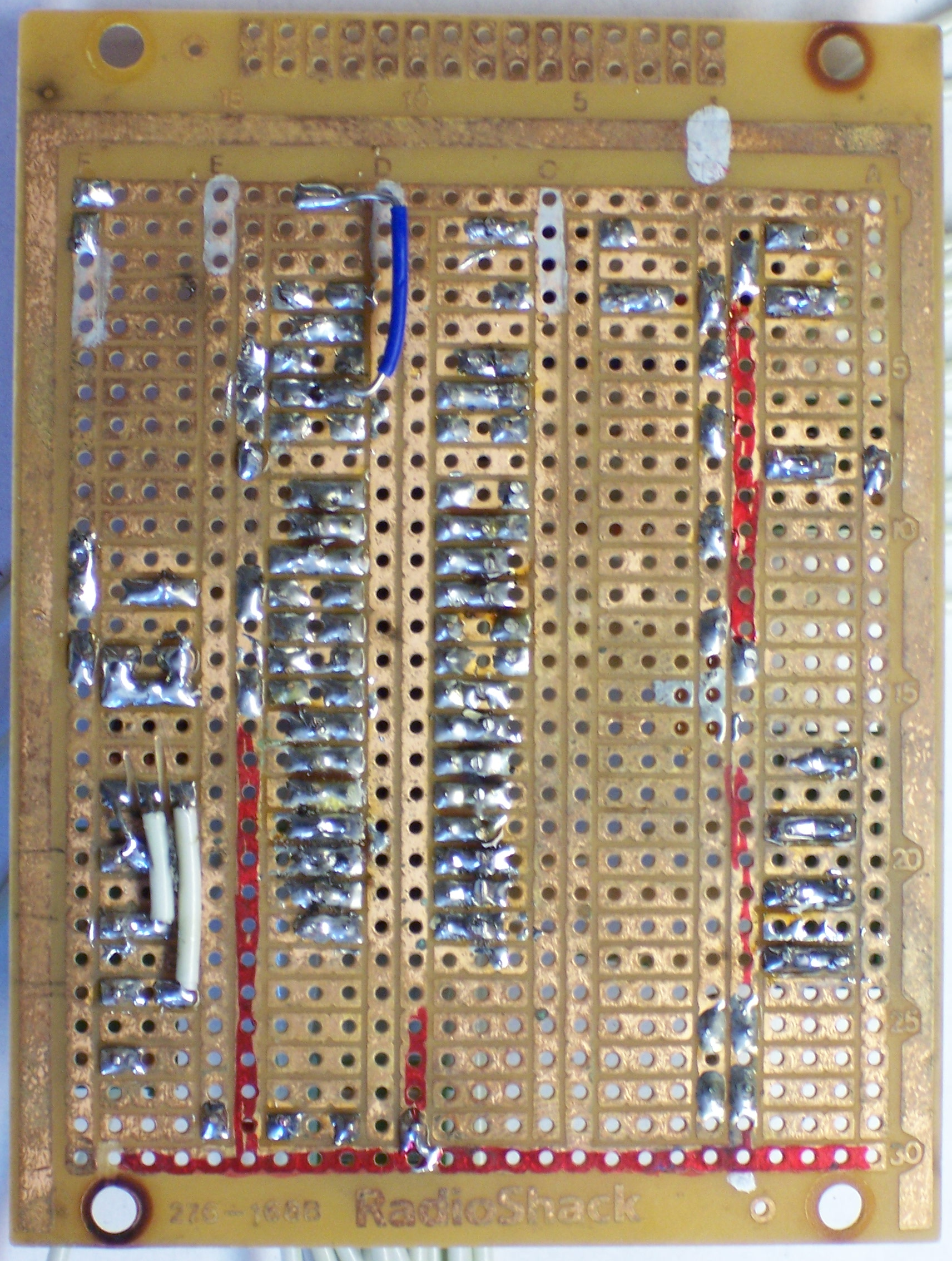
Once I had the parts placed, I turned to the back side of Steve’s board and began tracing connections. I added a connection on the schematic for each connection on Steve’s board, switching frequently to the PCB editor to draw out the physical path of the traces whose connections had been entered so far. I drew it as a double-sided PCB; where Steve had jumper wires on the top, I made a via and drew a top-side trace.
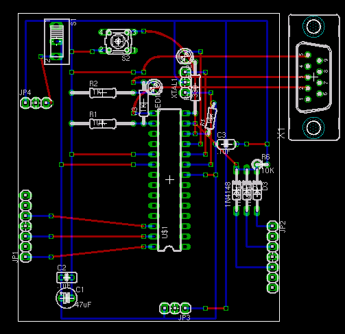
When I was finished, I had a fair facsimile of Steve’s board. Oh, there were some messy bits where jumpers overlapped and fly wires left the board, but it wasn’t too bad.
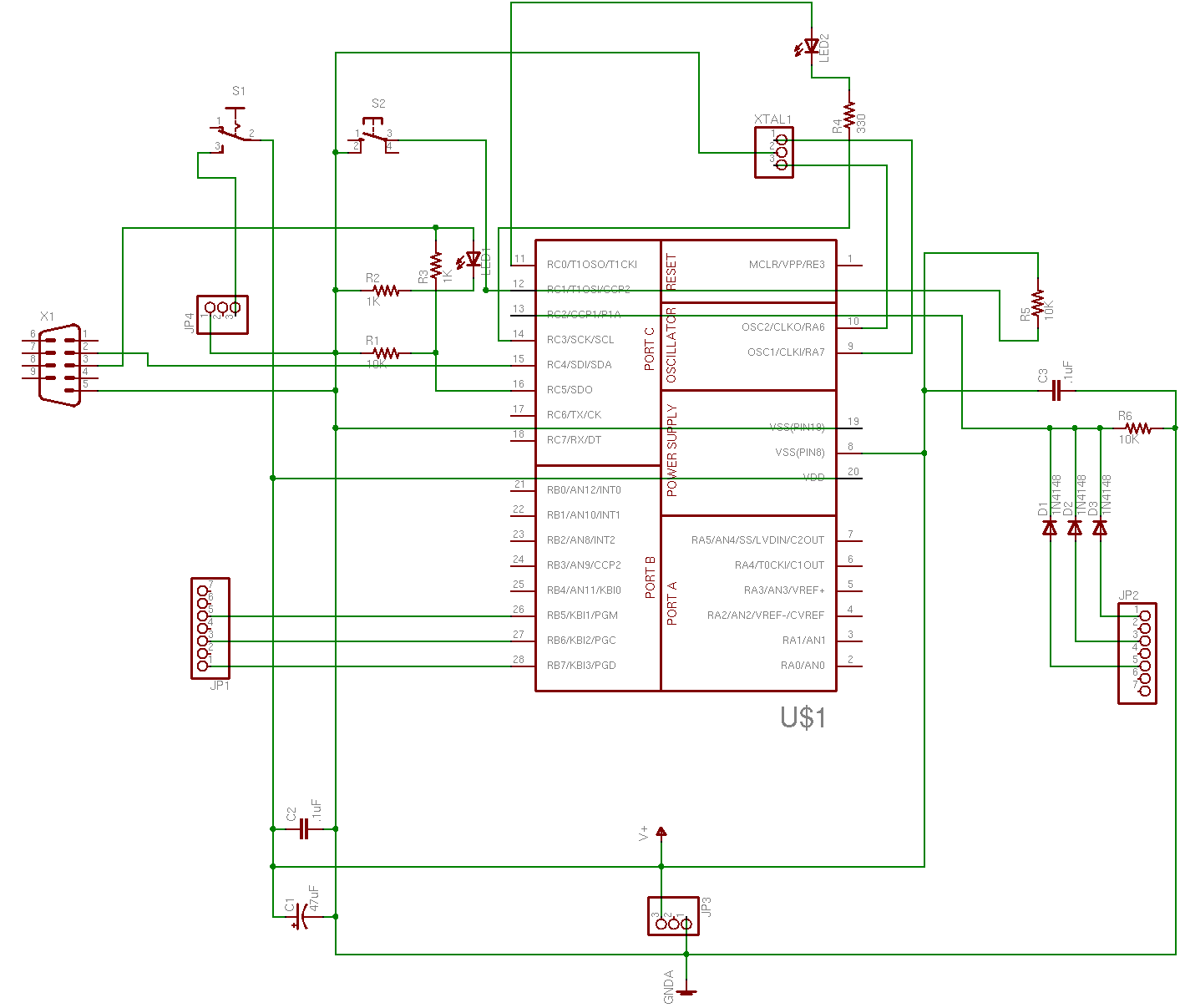
And more to the point, the schematic made it fairly easy to identify the problem. There are blocks of the circuit whose functionality isn’t identified (although it’s fairly easy to determine). But they’re not where the problem lies.
If you look closely at the power wiring to the PIC chip, you can see that it calls to have ground wired to pins 8 and 19 and V+ only to pin 20; but instead, ground is wired only to pin 19 and V+ is mistakenly wired to pin 8 in addition to pin 20.
Voila! Problem solved. Well, identified, anyway. I’ll leave it to Steve to rewire that.
Solder Splash
One more thing. When I was tracing the connections on LED2, the “run” light, I noticed solder splash between its upper pin and the ground bus. It’s at the right edge of the highlighted area, trying to hide underneath the blue jumper.
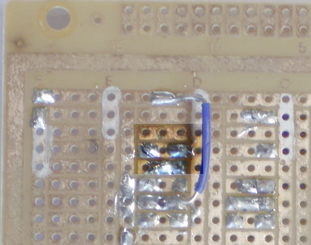
I haven’t checked it with a continuity meter, but it should be cleaned up to be safe. If I’m correct that it’s shorting the two wires, then the bicolor LED would still light one color (green or red) when port C3 (pin 14) is raised; but would remain dark when port C0 (pin 11) attemped to raise but was shorted to ground.
And with that, the board’s ready to go back to Steve.