Archive for the ‘LogoChip’ Category

LM34DZ Fahrenheit Temperature Sensor

Monday, February 2nd, 2009

This started as notes I made to myself long ago for the LogoChip, but they apply equally to the Arduino A/D converters.

The LM34DZ is a temperature sensor in a TO-92 case available from All Electronics for $2.50. It has the handy characteristic of reading an output voltage that directly corresponds to Fahrenheit temperature in a ratio of 10mV per °F. That is, at 70°F it reads 70 * 10mV = 700mV.

LM34DZ Fahrenheit temperature sensor

With a direct output voltage (rather than the varying resistance that many thermal probes provide), it’s perfect for hooking to a microcontroller A/D input. So, how to convert the A/D reading back into Fahrenheit temperature?

Well, the sensor reads 10mV (or .01V) per °F. Microcontroller A/D converters tend to have 5V input and read 1024 steps over the 0-5V range.

1024 steps / 5V ≈ 205 steps / V

So

(.01V / °F) * (205 steps / V) ≈ 2 steps / °F

Thus you can get a “maybe close enough” approximation with code like

tempF = analogRead(lm34Pin) / 2;

With a conversion error of +2.4%, this’ll get you within a couple of degrees at room temperature — close enough to make some macro-level observations about whether it’s getting warmer or colder for a physical computing project. Since the stated accuracy is only 1°F anyway, that’s not too bad.

If you need a more accurate conversion, you’ll need to use floating-point arithmetic if you have it (which the Arduino doesn’t [correction: does]) or find a fixed-point arithmetic library if you don’t. Or if your integer variables are large enough (at least 17 unsigned bits for temperatures up to 127°F, 18 bits up to 255°F), you can rearrange the order of calculation like so:

tempF = (1024 * analogRead(lm34Pin)) / 5;

Auto Power Sequencer for SAE A502 and A202 Amplifiers

Tuesday, August 7th, 2007

The project I’ve been working on lately is a power sequencer for my SAE A502 and A202 amplifiers. I bought my first A502 with summer job money when I was in college, and recently I’ve bought a few more on eBay. They’re big and beefy and I love ‘em.

My stereo rack, with Sony preamp and SAE amplifier stack

Their only drawback is that they have to be switched on and off manually — they’re not tied to my preamp. This is particularly annoying to my wife who hates all things electronic — she just wants to watch TV or a movie, and she has to fiddle with all these buttons to get the sound to come on.

Well, not any more.

Standby Circuit

Many of the SAE amplifiers, particularly including the “02″ series, have standby inputs. The SAE preamplifier puts out a signal telling the amplifiers when to turn on and off, and the whole stack is controlled by the preamp.

SAE amplifier standby input

Which is great if you have an SAE preamp and you just want to listen to stereo audio — but SAE went out of business long before the advent of home theater surround sound, much less 5.1 surround. If you want surround, you’re not using an SAE preamp; and if you’re not using an SAE preamp, you’re turning your amplifiers on and off by hand.

I’ve long dreamed of building a box to do that for me, and now I’ve done it.

The first step was determining how the standby signalling is done. The owner’s manual isn’t much help; it doesn’t list the details of the protocol, but only describes (in rather roundabout language) that you need to manually turn the amp on and let the preamp turn it off.

So I opened an amplifier and looked at its standby board. The circuitry is very simple, and I’ve since confirmed my schematic against the amplifier’s official schematic.

SAE amplifier standby circuit

The “input” and “output” jacks are identical and tied directly together, with the tips feeding the base of an NPN transistor. Put a small amount of current through the tip and the transistor will shunt the red wire’s voltage to ground.

Inside the amp, the red wire connects to the base of a Darlington pair that drives the main power relay. Steal its base current and the relay can’t switch the main power on; hence the standby is an override to keep the amp off, as the manual described.

Knowing that, it’s very simple to build a device to control the amplifiers.

Watching the Preamp

The question that remains is how to know when it’s time to turn on. In my case, since I have an A/V preamp, I thought the preamp put out a video signal any time it was on (even if it was just a bluescreen when no inputs are active). It turns out I was wrong, but this was still a productive train of thought.

I used an LM1881 video sync separator chip to watch a video connection. The chip ends up generating sync signals if none are present, so I couldn’t use its sync outputs to detect the presence of video; but it has a logic-level odd/even frame output that oscillates at 30Hz whenever an interlaced video signal is being received. Repeated rising (or falling) edges == video present.

LM1881 video detection circuit

I had already built and tested the circuit before I discovered that my preamp most certainly does not output video when it’s on, unless it actually has a video input on as well. That was very disappointing, since I don’t want the system dependent on a third device that supplies video — it should work whether I’m watching a movie, listening to a CD, or listening to 8-track.

Skulking around for alternatives, the best I could come up with was the switched outlet on the back of my preamp. I bought a slim 5V wall wart to plug into the back of the preamp and added another detection circuit to rectify and regulate an arbitrary low-voltage input.

Switched power detection circuit

The preamp powers up, the switched recep comes on, 5V feeds into the bridge rectifier, and a logic high feeds out. The input would do just as well detecting a low-voltage AC wall wart . . . if I had remembered to put a capacitor between the diode bridge and R4. Duly noted for the next version.

Control Logic

Cort was saying that I should have built the whole circuit out of discrete TTL logic, and I could indeed have done so, for a little retro charm. However, I wanted additional control that would have raised my chip count too high, so I built the control with a PIC.

When the preamp comes on, the sequencer turns on all four amps, one at a time, to spread out the inrush current. (Could have used a clock and a shift register.) But all four amps are only needed when watching movies — listening to music requires only the front and sub channels, not the center and rear. I wanted manual override pushbuttons so I could turn off the unused amps. (Could have used S-R latches.)

Additionally, when Cort and I were discussing what should happen to manual selections when the preamp eventually turns off, he suggested having a fully manual mode that ignores the signal detector inputs and heeds only the front-panel pushbuttons. (Could have . . . naahhhhh.)

Ultimately, I ended up using every available I/O pin on my PIC18F232:

  • 1 capture/compare input pin to watch the video signal
  • 1 input pin to watch the switched power signal
  • 2 output pins to run the bicolor power/mode LED
  • 4 input pins to watch the front-panel pushbuttons
  • 4 I/O pins to run bicolor amplifier status LEDs using the tristate trick
  • 4 output pins to control the amplifier standby inputs

I wrote the code in LogoChip Logo, with subroutines to service the input modules and a state machine to control the different modes. All of the timing is done in software, including the delay between turning on consecutive amps, and a loss-of-video countdown timer to keep short glitches from bouncing the amps.

Sequencer in Action

The video detector wasn’t a waste; I plugged a spare output of my DVD player into it, so the amps come on when the DVD player is turned on or the preamp is turned on, whichever comes first.

Here’s a video of me turning on the DVD player and the sequencer (just above the amp stack) turning on the amps, then turning off the DVD player and the sequencer turns off the amps after a delay. If you have audio turned on, you can hear the amps’ relays clicking in sync with the sequencer LEDs, then later clicks as the delayed speaker relays engage.

This is really slow to load; I’m working on migrating this to YouTube.

These are too slow to load and are causing problems with my browser. You’re welcome to paste in the URL and try them if you like.

embed src=”http://www2.neufeld.newton.ks.us/images/electronics/2007/08/06/100_3046.mov” controller=”true” width=”480″ height=”656″ kioskmode=”false” autoplay=”false” pluginspage=”http://www.apple.com/quicktime/download/”>

There’s one little snag — the standby circuit on my top amplifier isn’t working, so I’m still turning it on and off manually. I just bought an SAE preamp on eBay and should receive it within a week or so, at which point I’ll hook it up and see whether it has magic juju that my sequencer doesn’t, or whether I need to troubleshoot my amp.

Here’s a nearly identical video of me turning on the preamp and the sequencer turning on the amps.

embed src=”http://www2.neufeld.newton.ks.us/images/electronics/2007/08/06/100_3047.mov” controller=”true” width=”480″ height=”656″ kioskmode=”false” autoplay=”false” pluginspage=”http://www.apple.com/quicktime/download/”>

Kits for Sale

Well, not yet, but I’m interested in pursuing it. There’s a pretty active community of SAE equipment owners, and I have to believe there’d be other folks in the same position, using SAE amps with non-SAE preamps. After I work through a few issues, I’d like to offer the power sequencer in both kit and appliance form and see if I can sell a few.

I want to split the main circuit board into a front-panel board and a control board, to make it easier for other folks to adapt the LED and button spacing to fit enclosures of their own choice. That also solves the problem with the RJ-45 jack, as it could then be on the component side of the control daughterboard. And I made some mistakes in the physical size and mounting of the board that I’d like to correct as well.

Once I touch up the circuit and board designs and clean up my code, I want to release the whole schmear under a Creative Commons license, probably Attribution Share Alike. Lady Ada’s Creative-Commons-licensed kits are pretty inspiring to me, and I’d like to think there’s a small but healthy market for kits and appliances that don’t rely on keeping the design closed and secret.

Wish me luck!

PCB Layout and CNC Drilling Problems (and Solutions)

Monday, August 6th, 2007

I recently finished the prototype of my latest project (to be described in an upcoming post), and I made a lot of mistakes in PC board layout and construction. Like the SparkFun gallery of prototypes, I thought it was worth describing my problems and their solutions, to help myself and others avoid them in the future.

I’m doing that in two forms: a couple of detailed blog posts, and a new page with a summary version of the solutions. In the blog form, I’ll describe the problems in the order I encountered them; on the tips page, I’ll list the solutions in the order they’d be used when doing it right the first time.

Fitting the Case

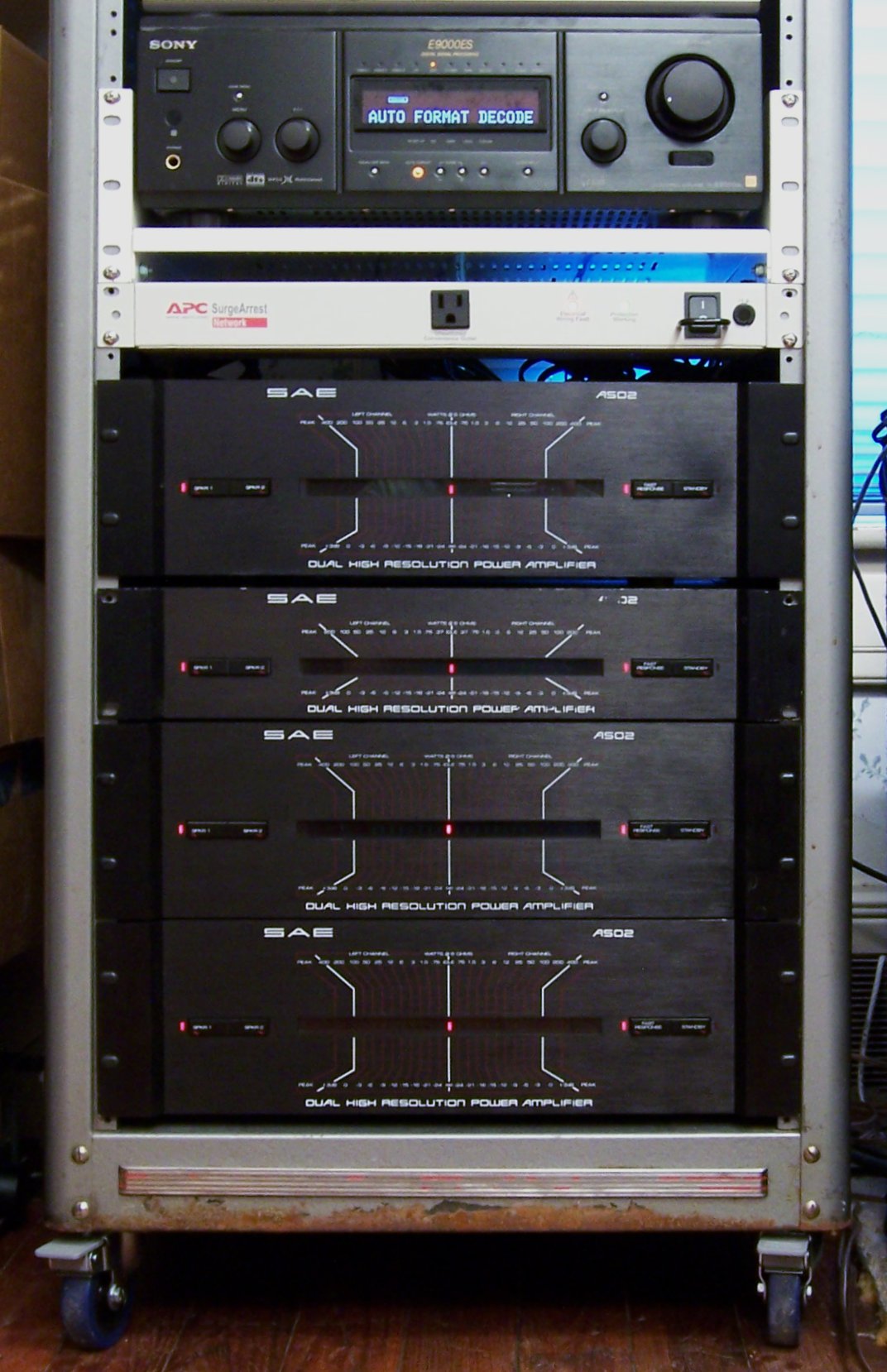
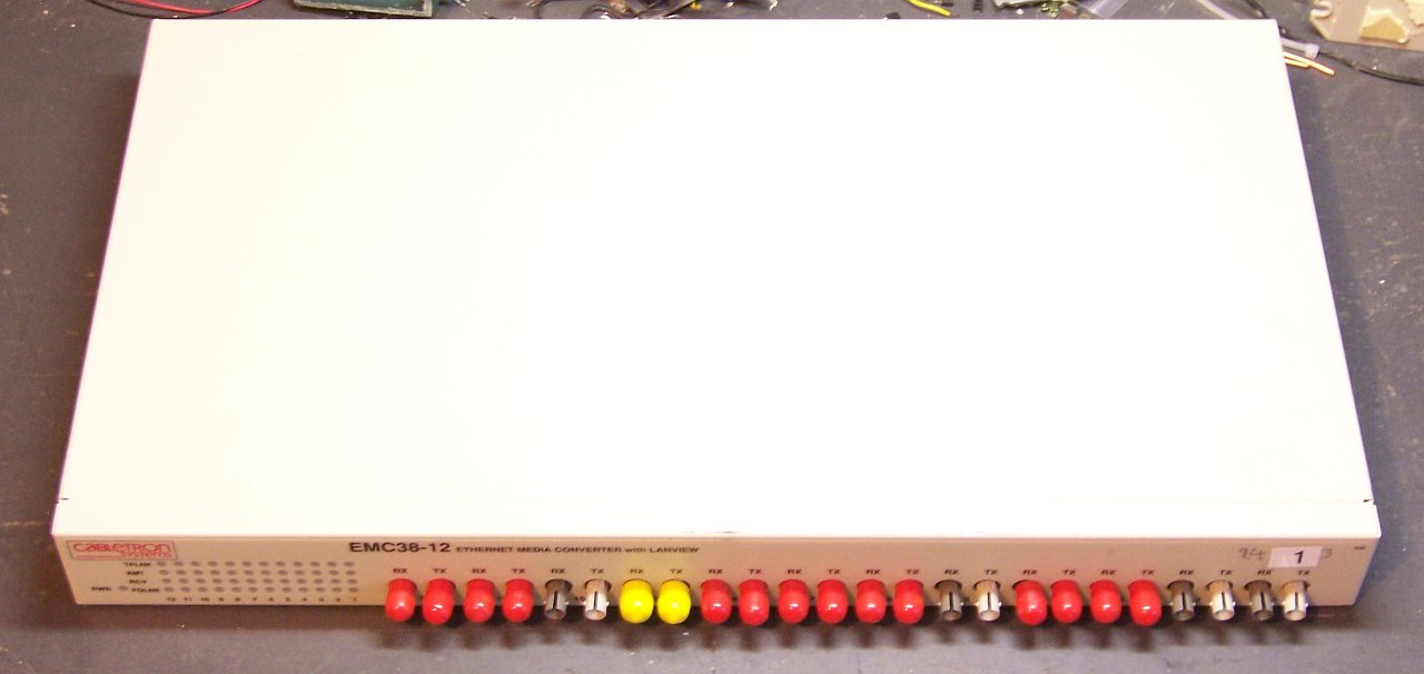
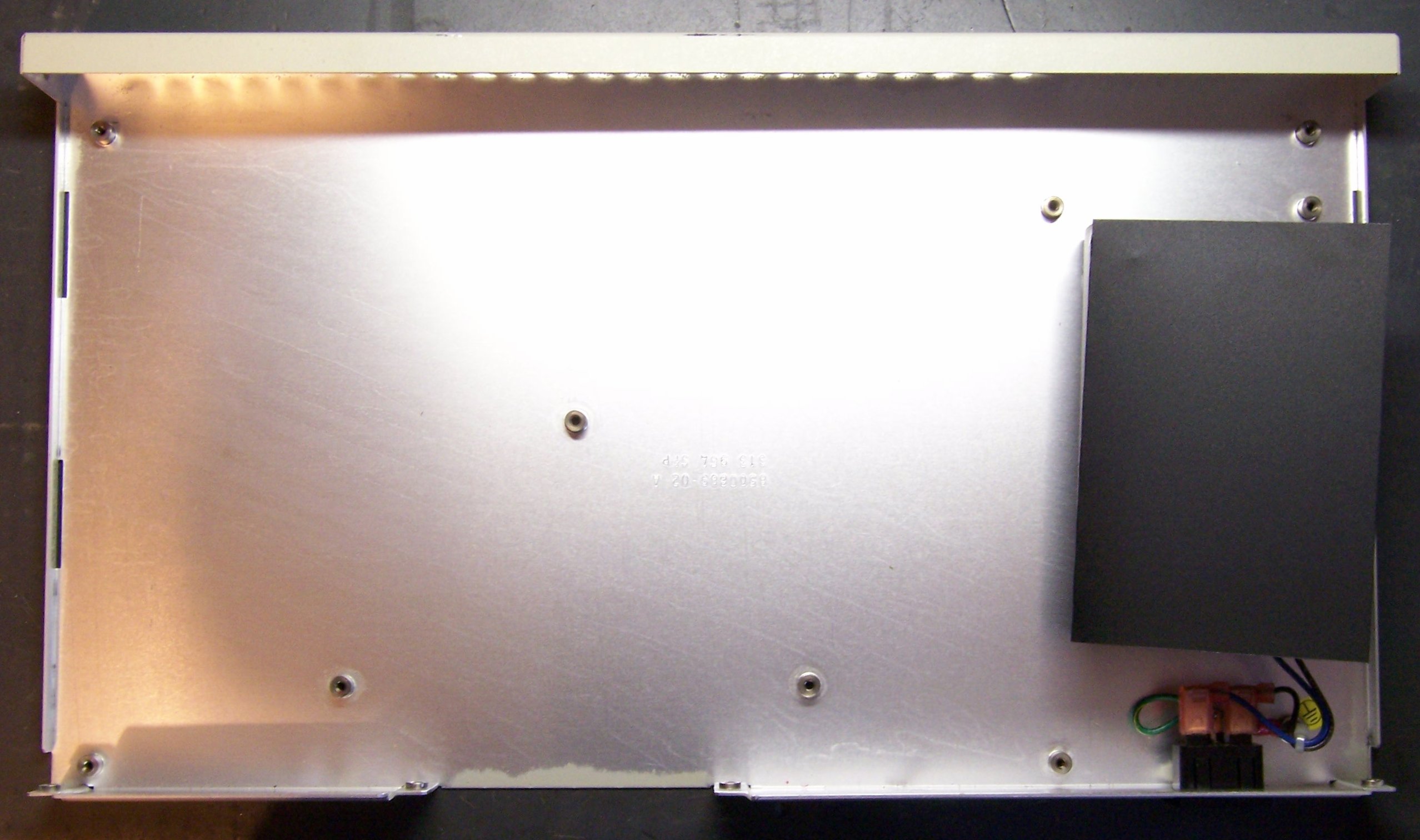
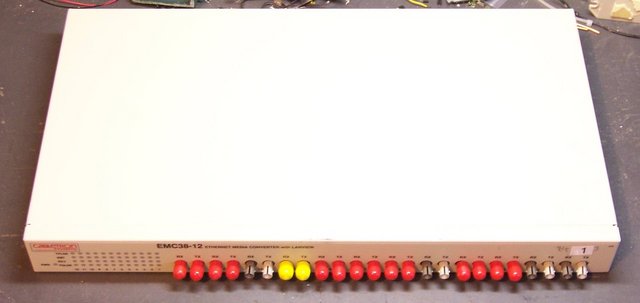
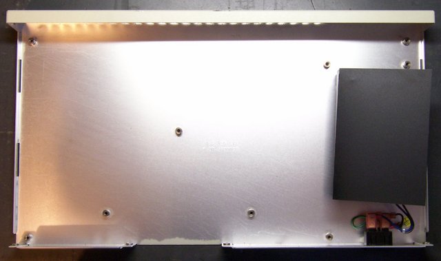
The project I’m building is a control device for my stereo system, so I wanted to build it in a rackmount case. Rackmount project boxes seem to be inordinately expensive ($40+); so for the prototype, I salvaged a piece of dead network equipment (rackmount 12-channel 10M fiber-to-copper media converter), ditched the guts, and kept the case. The power supply was on a separate board and turned out to be 5V, so I left it in place to drive my circuit.

Rackmount fiber to copper media converter

Empty rackmount case with power supply

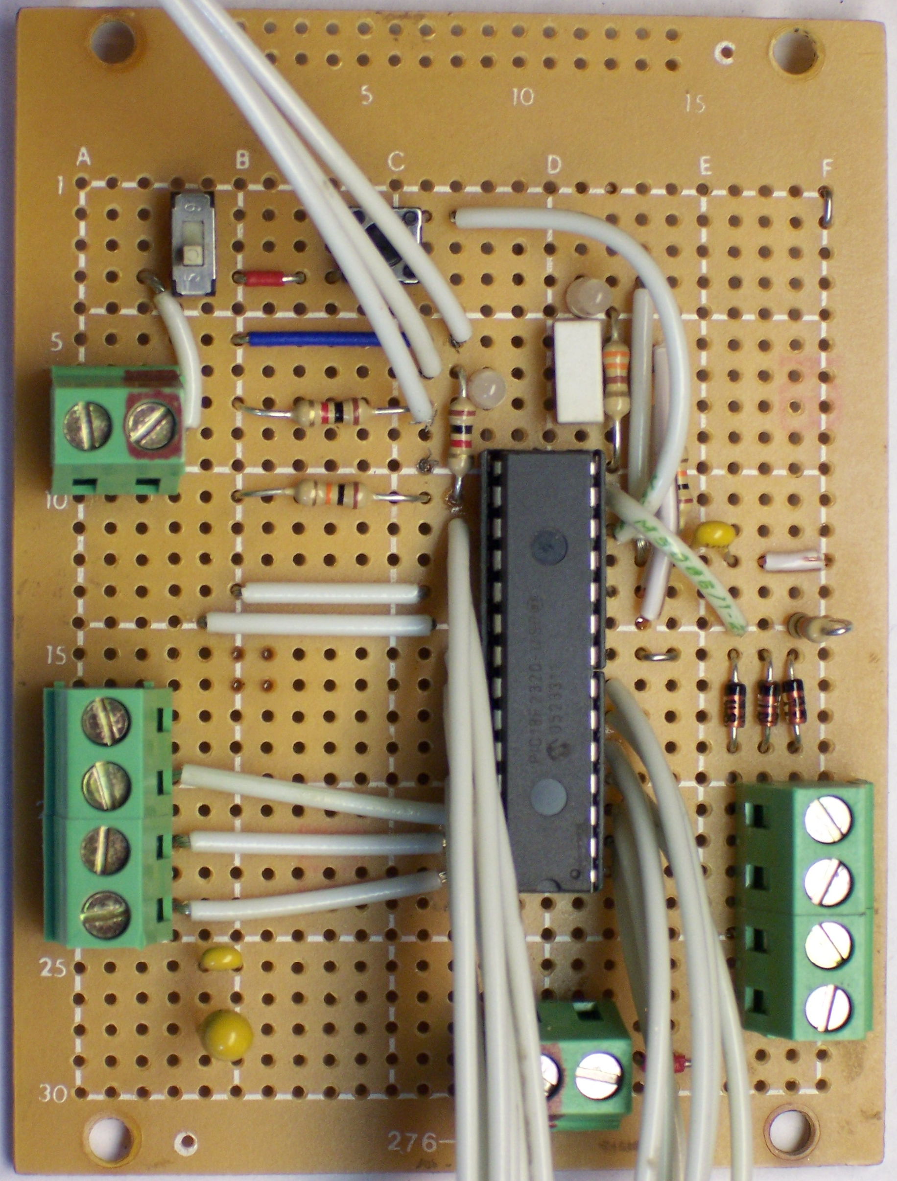
I needed pushbuttons and indicator LEDS on the front panel, so I planned my PCB to mount behind and parallel to the front of the enclosure. I measured the outside of the case and subtracted a generous .1″ from each edge to account for the thickness of the metal and to provide clearance around the edges of the PCB.

For the prototype, I decided to use the existing holes in the front panel for my LEDs and pushbuttons. I measured their approximate distances from the lower left corner and placed the components in the PCB layout program accordingly.

First mistake: When I measured for the size of the PCB, I didn’t look closely enough at the case. Where the top cover fits into the front edge of the case, there’s an extra lip underneath. I made the first board layout too tall to fit.

Lesson: Don’t make assumptions about the fit of the case. Inspect and measure where the PCB will actually fit.

Fortunately, before making a board, I printed the silkscreen layer and board outline from the layout software (FreePCB), cut and taped the pieces together, and held it inside the case to test the fit. I realized my error at that point, and correcting it was a (relatively) simple matter of changing the board outline and moving components and traces. I also tweaked the positions of the LEDs and pushbuttons for a better fit with the front-panel holes.

Auto Power Sequencer, top silk screen layer

Lesson: Print the board design on paper to test-fit into the enclosure before making a real board.

Challenges of a Single-Sided Board

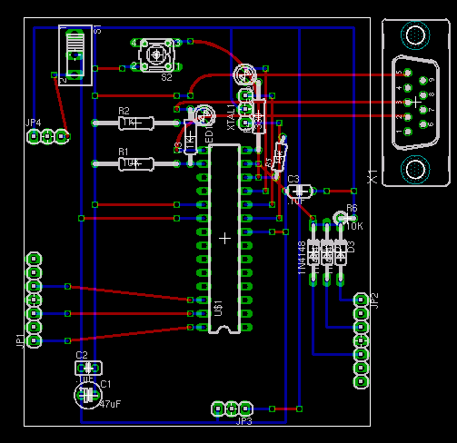
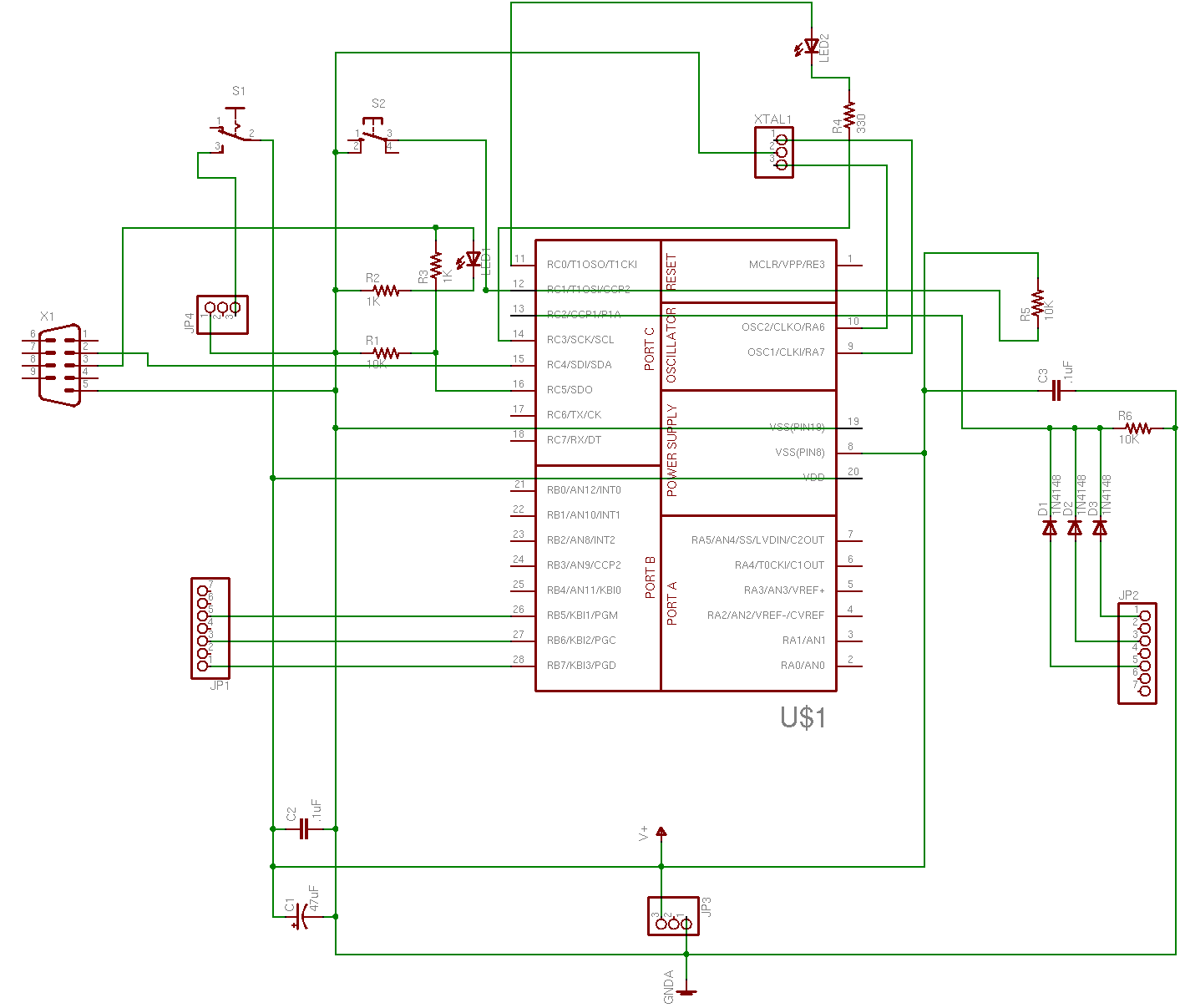
I could have designed most of the circuitry using 7400-series digital logic, but some of the override functions I wanted to provide on the front panel would have got tricky, so I used a PIC microcontroller running the LogoChip language.

In order to perform firmware updates, I needed to include a serial port, but I didn’t really want to clutter the back panel with something that would be used so infrequently. For my own use, I like connecting with what I affectionately call a “Cisco blue cable,” the DB-9 to RJ-45 serial cable that ships with every piece of Cisco equipment (so I have a carton full of them). That meant putting an RJ-45 jack inside the case, and the problem was where to put the jack.

LogoChip in Altoids tin

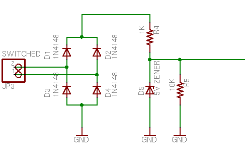
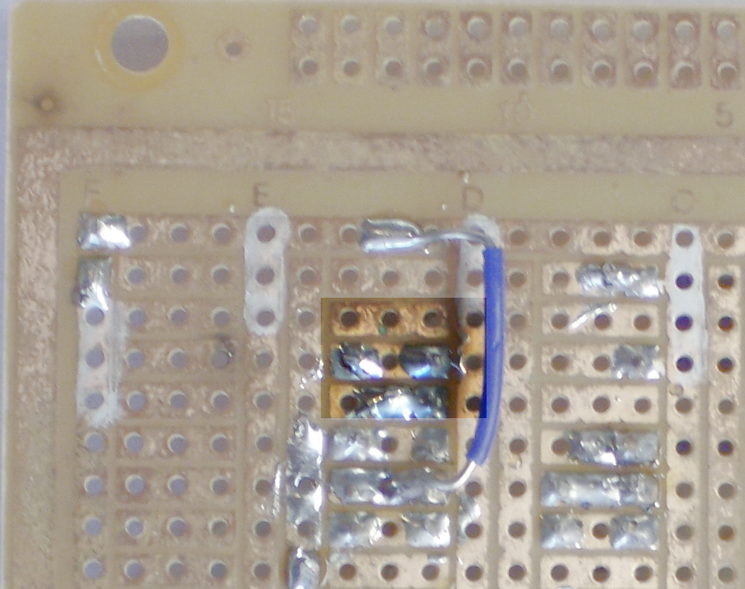
Normally a jack would mount on the component side of the PC board, like the one up against the battery in my Curiously Strong LogoChip case, but here the component side was going to be pressed up against the inside of the front panel. Not only would that make the jack inaccessible (buried between the PCB and the front panel), but the jack was taller than the mounting hardware I wanted to use, and would have pushed the board too far back from the panel.

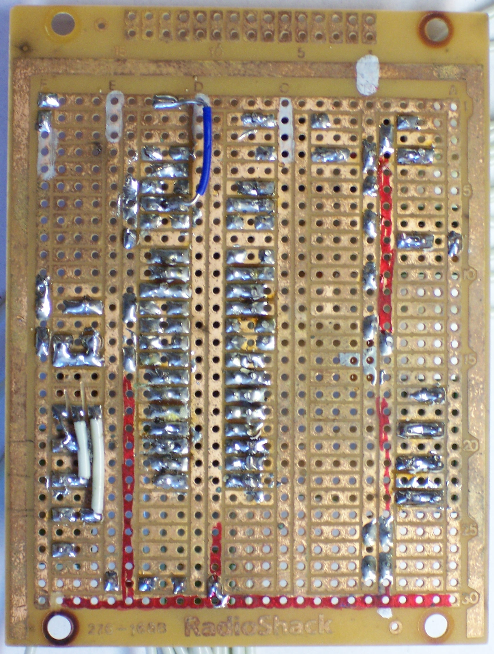
On a double-sided PC board, I could have mounted the jack on the “back” side and soldered it from the top. On my single-sided board, though, I’d have no way to solder it to the back-side traces — the jack itself would occupy the same space the soldering iron needed to.

Auto Power Sequencer, serial board

I decided to settle for making a very small daughterboard, just big enough for the jack and supporting components, to mount to a spare post in the bottom of the case. I wasn’t wild about the idea, but at least it’d get me by. In fact, I ended up scrapping the serial board idea and hooking up a temporary jack, for reasons I’ll describe later.

Lesson: Plan ahead for bulky components.
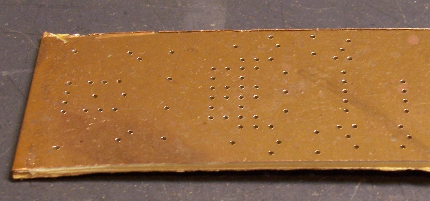
Drill Bits

Once I (thought I) had the board design finalized, I generated an Excellon drill file to take to Joel’s house and drill on his CNC machine. Because his machine has only about 12″ of travel and I needed to drill a 16.8″ panel, I needed to split the holes into two sections, so I could rotate the board halfway through and resume drilling from the other end.

To do this, I picked a spot to divide the board where I had a relatively long run of traces with no holes nearby. That way, inevitable alignment problems could be corrected by slanting the traces from both sides to meet in the middle.

I wrote a set of scripts for selecting, rotating, translating, and mirroring hole data in Excellon drill files. (I’ll post these after I clean them up a bit.) I also wrote a script to remove Excellon tags that Joel’s DanCAM software doesn’t recognize. (I had earlier created a drill export specification to generate DanCAM from EAGLE, but I was using FreePCB due to the larger board size.) I wrote up a nice Makefile to control the whole process, so I could export new drill files and just run make to get the new copies for Joel’s machine.

I cut a strip off my giant PC board from Slim, cut a couple of sections to length, and went over to Joel’s to start drilling. I decided to drill the boards copper-side-up, so I’d have less tear-out to sand off afterward.

PCB board with drilled holes

Lesson: Drill with the copper side up. It leaves perfectly clean holes that don’t need sanding.

I drilled the first board, and half of the third board, as a top-to-bottom mirror image of the correct hole placement. I drove back and forth across town to get more boards way too many times.

Lesson: Check drill file mirroring very carefully, to make sure it matches the placement of the board on the drill table.

I also ended up breaking something like four bits, mainly due to operator error. In the CAM software, you enter the heights of the Z axis with the drill bit up (out of the board) and down (drilled into the board). At one point, I miskeyed the up position lower than the down position, causing the machine to move the table with the bit lowered into the board. Snap. I always do a dry run before letting it drill the whole board, but it had already dived into the table before I could abort.

The machine was also drilling fairly aggressively for the size of bit I was using, resulting in the breaking of another bit. I slowed it down and didn’t break any more after that (I think).

Lesson: Be aware of CNC machining parameters, particularly those relating to position and speed.

But I didn’t start out with very many small drill bits, and each time I broke the smallest remaining one, the holes I was drilling got larger and larger. By the time I got the board finished with all the holes in the right place, I was using a 39-mil drill bit, which was way larger than I wanted — way larger than my component leads.

drill bit

Lesson: Stock up on appropriately-sized drill bits.

I’ve since placed an order with Drill Bit City for a couple of 25-packs of 5 each even sizes #72 – #64.

Drill Path

The hole list in the Excellon drill file isn’t in any particular physical order — the hole order probably has to do with the order the parts were imported into FreePCB from the partlist. DanCAM has an optimizing stage to reorder them into a more optimal path for the slow machine to travel, but I’ve noticed in the past that its idea of optimal seemed really strange and . . . suboptimal.

This time, I caught on to what was happening. DanCAM (at least the way we’re using it) doesn’t support changing drill bits to drill different-sized holes, so I drill all the holes with the same size bit. But internally, it’s still paying attention to the drill size, and optimizing each different bit’s path as a separate pass across the board, resulting in much unneeded movement when drilling with a single bit.

I updated my FreePCB Excellon to DanCAM conversion script to reduce the drill rack to a single size bit, and the next optimization and drilling operation went much faster than before — so much so that it felt like a qualitative rather than merely quantitative difference in drilling speed.

Lesson: If you’re drilling all the holes with the same size bit, make sure the machine knows that.

Having optimized the drill path so much better than before, I noticed that the machine was occasionally drilling the same hole more than once. I knew immediately why that was: Due to a quirk in the way FreePCB routes traces, there were numerous places on my board that I had multiple logical vias at the same physical location.

I wrote a very simple drill-uniq script to remove duplicate holes:

my %seen;

while (<>) {
    next if /^X/ && $seen{$_}++;

    print;
}

And the drilling operation got faster yet.

Lesson: Eliminate duplicate holes from the drill file, if the CNC machine isn’t smart enough to do it for you.

CNC Stepper Speed

My PC board production sequence is to drill the holes with the CNC machine, then print and iron on a toner transfer, then etch away the visible copper with ferric chloride. For the iron-on process to work, the predrilled holes need to align exactly with the printed copper trace pattern. I’ve noted in the past that they generally don’t align across the entire length or width of the board, and attributed that to inaccuracies in the paper feed rate of my laser printer.

This time, while I was waiting for one of several iterations of board to be drilled (due to my continuing errors), I checked the registration of the previous iteration and found it to be so bad that I got a ruler to find out exactly where the error was. It turns out that the answer was both — the drill and toner spacing were both wrong. Holding two iterations of drilled PCB up to the light revealed that the drill wasn’t even consistent from one pass to the next.

Since it’s a CNC drill, the only way that should be possible is if the steppers are skipping steps. If you push a stepper motor too fast, it skips (lags) a little bit, and stays out of sync until the next time you send it to the home position to check where it is. DanCAM’s setup process includes tests to make sure the motors are staying synchronized, but it’s pretty hard to tell if they’re losing only a few steps.

I went through the motor speed calibration section again, which boils down to running the motors faster and faster until they’re obviously losing steps, then backing off the speed until they seem stable again. I backed the speed off further than before, and on the next drill pass got all the holes as close to where they belonged as I was able to measure (except three that just randomly went a little bit off — still don’t know why, but I don’t think it was lost steps).

Lesson: Make sure the feed rates are within the steppers’ and drivers’ capacity.

At this point, I finally had a board that fit into my enclosure, with all the holes drilled (pretty much) where I wanted them. And a lot of things to remember to do better the next time.

Debugging a LogoBoard

Wednesday, April 18th, 2007

After the 2006 Technology: Art and Sound by Design final exhibit, Steve Atwood worked on building his own LogoBoard to use in his sculpture. He found that his board wasn’t working and was overheating, and asked for my help troubleshooting it. To my recurring shame, I’ve had his board ever since with very little progress to show for it. Time to rectify that.

The Board, the Symptoms, and Initial Efforts

Steve Atwood's LogoChip prototyping board

Steve built his circuit on a prototyping board with a .1″ perforated .1″ grid and connecting traces on the back, much like a solderless breadboard. The PIC microcontroller is in the center, with various components, connections, and wires surrounding it.

The main thing I knew when Steve gave me the board was that the LogoChip was overheating. I measured the resistance from the LogoChip’s power pin to ground pin and got some very low value like 4Ω, so I knew something was broken, but not dead shorted. I replaced his chip with one of my own and tested again; mine overheated and had the same resistance as well, so his problem wasn’t just that his chip had burned out.

And there it sat for a year.

Drawing the Schematic

In order to do any further debugging, I needed to determine and draw out exactly what was connected where, so I could examine the schematic and find what looked amiss. And the easiest way I’ve found to make a schematic from a PC board is to recreate the circuit in design software, building out the schematic and a reproduction drawing of the physical PC board at the same time. When the traces on the board drawing match the traces on the board, the schematic is correct and complete.

Working with two windows in EAGLE, I created a new project and added all of the components from Steve’s board. I had to fudge on the screw terminals and the crystal oscillator because I didn’t have library parts for them; but for a quick job like this I feel okay substituting a .1″ header and simply remembering what’s really going on. I carefully placed each component on the PCB diagram at the exact space corresponding to its placement on the real board.

LogoChip prototyping board, back side

Once I had the parts placed, I turned to the back side of Steve’s board and began tracing connections. I added a connection on the schematic for each connection on Steve’s board, switching frequently to the PCB editor to draw out the physical path of the traces whose connections had been entered so far. I drew it as a double-sided PCB; where Steve had jumper wires on the top, I made a via and drew a top-side trace.

PCB layout of Steve Atwood's LogoBoard

When I was finished, I had a fair facsimile of Steve’s board. Oh, there were some messy bits where jumpers overlapped and fly wires left the board, but it wasn’t too bad.

Schematic of Steve Atwood's LogoBoard

And more to the point, the schematic made it fairly easy to identify the problem. There are blocks of the circuit whose functionality isn’t identified (although it’s fairly easy to determine). But they’re not where the problem lies.

If you look closely at the power wiring to the PIC chip, you can see that it calls to have ground wired to pins 8 and 19 and V+ only to pin 20; but instead, ground is wired only to pin 19 and V+ is mistakenly wired to pin 8 in addition to pin 20.

Voila! Problem solved. Well, identified, anyway. I’ll leave it to Steve to rewire that.

Solder Splash

One more thing. When I was tracing the connections on LED2, the “run” light, I noticed solder splash between its upper pin and the ground bus. It’s at the right edge of the highlighted area, trying to hide underneath the blue jumper.

Solder splash on prototyping board

I haven’t checked it with a continuity meter, but it should be cleaned up to be safe. If I’m correct that it’s shorting the two wires, then the bicolor LED would still light one color (green or red) when port C3 (pin 14) is raised; but would remain dark when port C0 (pin 11) attemped to raise but was shorted to ground.

And with that, the board’s ready to go back to Steve.

CdS Photocell

Tuesday, April 17th, 2007

A cadmium sulfide (CdS) photocell is a passive component whose resistance decreases when light shines on it. CdS photocells can be used to detect when lights turn on, to orient things toward a light source (electronic sunflower), and to detect shadows passing across them.

CdS photocell

To use a CdS photocell, you put it in series with a resistor and put a voltage across them. This forms a voltage divider: the voltage at their junction is determined by the proportion of the two resistances. If you want brightness to increase the measured voltage, put the photocell on top; if you want darkness to increase the measured voltage, put the photocell on the bottom.

Circuit diagram showing two ways to connect a photocell

All that remains is to determine an appropriate value for the complementary resistor. Assuming you want output voltage to increase when brightness increases, the goal would be to make the output read as close to 0V as possible when it’s as dark as you expect it to be, and as close to your maximum voltage as possible when it’s as bright as you expect it to be.

To begin this calculation, I measured the resistance of the photocell (out of circuit) in light and dark conditions. With the photocell shown above, I found the following values:

450KΩ in the dark (my finger pressed over it)
36KΩ in average light
7.6KΩ in bright light (under my fluorescent desk lamp)

I discovered later that the photocell’s carrier PCB isn’t entirely opaque and a noticeable amount of light does leak in around the edges even when the face is covered. The resistance in true darkness would probably be even higher.

I decided to scale the photocell’s circuit to the range from darkness to normal room lighting, so calculating for a resistance range of 450KΩ to 36KΩ. Because this is only a single order of magnitude variation of resistance, I could already tell the voltage swing of the output wasn’t going to be as large as I’d like. I picked a 100KΩ resistor and estimated the voltage range:

5V * (100KΩ / (100KΩ + 450KΩ)) ≅ .91V
5V * (100KΩ / (100KΩ + 36KΩ)) ≅ 3.7V

So it has a swing of about 3V out of a 5V range. Not ideal, but it still provides a fair amount of resolution.

Finally, I connected the photocell to my LogoChip’s A0 input and confirmed its behavior by running print read-ad 0. I got a wide range of values out of the A/D converter, making this circuit quite usable for microcontroller interfacing.

I also posted a cookbook version of using the photocell on the TASD class wiki.

Making Googly Eyes, Part 2: Construction

Monday, April 16th, 2007

As noted in Googly Eyes Part 1, I built a demo back in February out of a CD-ROM drive optical sled assembly and a couple of ping-pong balls. In the earlier installment, I discussed reverse-engineering the sled’s electrical connections; now here’s how I rebuilt it to operate eyeballs.

I had thought I might find some googly eyeballs in the Wal-Mart craft department, for making big puppets or something. But all their googly eyes were the flat, button-like kind that just stick onto a surface, so I went with my fallback plan of ping-pong balls.

Drawing an eye on a ping-pong ball

I drew an eye onto two of them, with a black pupil and green iris. I didn’t mean to get the iris quite so dark, but at least I made it with radial lines.

Googly eye with bolt for axle

I located and marked the north and south poles of the ping-pong ball as carefully as I could, then drilled through with PCB drill bits. After stepping through several increasing sizes, I was able to use my stepped drill bits to make nice, round, even holes for the axle. I stuck a bolt through and threaded a nut up fairly close to the ball, so it could swivel but not move up and down much.

Googly eyes mounted to frame, front view

The sled assembly didn’t have the right sized holes in the right places, so I used big fender washers to make things fit. The eyeball-mounting nut is tightened against the fender washer, with another washer and nut on the bottom side. The bolts continue through the frame and act as legs to raise the underside of the carriage off the surface it’s sitting on, with cap nuts (acorn nuts) for feet to keep the end of the bolt from scratching.

This was actually a bit less than ideal, because the mounting hole for the right eyeball (left edge of the picture) is in a section that’s bent up and raised above the plane of the other holes. I tried compensating for the height difference with an extra nut under the left eyeball, but it’s still not quite right. Probably a washer in between the two nuts would fix it up.

Fully-assembled googly-eyes mechanism, top view

Finally, I needed to translate the sled’s linear motion into the eyeballs’ rotary motion. I turned a loop into the end of a couple of pieces of stiff wire, and . . . had to take the eyeballs back apart again. I drilled another hole in the back of each one, then pushed the wire loop into the interior and reassembled them with their bolts going through the wire loops. Once reassembled, I dabbed some hot glue where the wires came out of the eyeballs; now I could use the wires as control rods to rotate the eyes.

I removed all the optical parts from the carrier sled, then ran a bolt up through it to the height of the eyeballs. I made a loop in the center of another piece of wire and sandwiched it between two nuts on the sled bolt, then made a loop at each end around the eye control rods. After a little tweaking of the angles, I got it set up for fairly smooth movement, with the ends bent to keep things from slipping out of the loops.

In Part 3, I’ll discuss the software that moves the motor and watches the optical disk to monitor travel.

PWM Control of a Larger DC Motor

Saturday, April 7th, 2007

A year or two ago, I bought a couple of cheap cordless drills at Harbor Freight with thoughts of tearing them down to use the motors for MOSFET-controlled robot drive systems. Yesterday in lab, several guys were talking about how to control DC motor speed for their final project. Serendipity kicked me in the butt and got me prototyping.

The Circuit

The obvious approaches to varying DC motor speed are varying the supply voltage and varying a resistor in series with the motor (which amounts to the same thing). The problem is, DC motors don’t run well on a low supply voltage, and the response is very non-linear.

The usual solution is to use pulse-width modulation (PWM): turn full power to the motor on and off rapidly, increasing (modulating) how long the power is on (pulse width) to increase the motor speed, and decreasing the pulse width to decrease the motor speed. And the PIC (the underlying hardware of the LogoChip) has built-in PWM control, because it’s designed to be used for a wide variety of applications just such as this.

The LogoChip/PIC can’t supply enough power to drive a large motor, so the total control circuit involves a LogoChip, a MOSFET power transistor, and some “glue” circuitry to interface the two together.

MOSFET motor speed control schematic

If I’d been building the circuit on a breadboard, I’d probably have started by plugging in components and wiring them up, because mistakes are easy to correct by unplugging and replugging. But since I was using larger components that I was going to need to solder, I didn’t want to have to change too many connections; so I started by drawing the schematic I intended to build.

(First I reread my May 2006 post about driving stepper motors with MOSFETs. They don’t use the same circuit, but I had taken the time to review my textbook and figure out how to treat MOSFETs right; and my blog isn’t just for y’all–it’s secondary storage for my own memory.)

The PIC’s PWM output is on port C2. The MOSFET’s gate needs at least 7V to saturate (turn all the way on), so port C2 controls the base of an NPN transistor (any common NPN will do; I happened to have a 3903) that switches the MOSFET gate between 12V and ground. The N-channel MOSFET in turn provides a ground path to turn on the motor when the MOSFET’s gate voltage is high.

The only snag is that the bipolar transistor inverts the control logic; so when C2 is high, the motor is off; and when C2 is low, the motor is on. Oh well. We’ll compensate in software.

Wiring it Up

I started by bolting one of my IRF510 MOSFETs to a heatsink. I should have used thermal grease, but I didn’t have any handy and I’m doing a quick test. And I should have used an insulator (since the FET’s tab is wired to drain, and that’s not going to be ground, and the heatsink might bump into something that’s grounded), but the heatsink seems to be anodized and sorta insulated already and I’m just doing a quick test.

MOSFET mounted to heatsink

I could have used the cordless drill’s battery to power the motor, but I didn’t feel like rewiring that much of the drill right now. So I settled on using my trusty old PC power supply–and I desoldered a connector from a dead CD-ROM drive to mate with the power supply. (Bench vise, heat gun, and pliers.)

Molex power connector on CD-ROM drive board

I wired the MOSFET to the power connector and left fly wires to go to the motor and the LogoChip. As always, I put heat-shrink tubing on each solder joint to be safe. The 10K pull-up resistor at the end of the blue wire, hidden behind the yellow wire next to the power connector.

Fully-wired MOSFET and power connector

The 5V supply on the power plug isn’t needed, so I insulated it as well.

Connecting the Drill

The largest DC motor that I could think of having at home was the cordless drill. It’s not as big as the windshield wiper motor that Team Doccia might be using, but it’s the best I could do. Here’s the victim with its the case removed:

Cordless drill, case opened

The motor is the silver and white cylinder in the center of the top of the picture. The tan cylinder to its right is the planetary gear system that reduces speed and increases torque.

To the left of the motor, you can see the MTP15N06V MOSFET that normally runs the drill. I could have reused it, but (1) then I’d have been done before I even started; and (2) I wanted to test with a FET that I had lots of, so someone else could use exactly the same circuit. Both the drill’s MTP15N06V and my IRF510 have a built-in reverse-biased diode to shunt the back-EMF spike that occurs when the supply voltage is removed from an inductive load (like a motor).

Cordless drill motor rewired for MOSFET speed controller

I pulled the the motor out of the drill casing, soldered on the leads from the FET wiring harness, and jammed it back in. I could have laid in on my bench for testing, but I was afraid the counter-torque when the motor started up at high speed might roll it right off the edge. The gearbox has a tab on the bottom that mates with the case and keeps it from twisting.

LogoChip Wiring

Tom left a nice prototyping area on the LogoBoard when he designed it, so I built the rest of the circuit there. I soldered a header socket into the connector for pin C2, plugged the NPN transistor into the breadboard section, and plugged in the base resistor and the gate and ground leads from the FET assembly.

LogoChip NPN switching circuit

Here’s what the whole works looks like when it’s all hooked up:

Cordless drill motor wired to MOSFET speed controller

Control Software

For prototyping, I reused my old motor-pwm-demo.txt program, even though it has some extra stuff that’s not needed here. I called pwm-init and then pwm-set 255 255 to shut the motor off. (Remember, it’s backwards logic because of the inverting effect of the NPN switching transistor.) pwm-set 255 0 turned the motor on at full speed, and pwm-set 255 128 selected a medium speed. pwm-set 255 196 was about as slow as it could reliably go.

To explain the code, the first parameter (the one that I’m always calling with 255) is the period of the control pulse–the higher the number, the longer between consecutive pulses (i.e. the slower the pulse train). The second parameter is the pulse width–how long each pulse output should be on. So pwm-set 128 64 should have about the same effect as pwm-set 255 128, only twice as fast (half as long).

Unfortunately, that ain’t quite so. Due to the inductive effects of the motor coils, some frequencies of PWM control work better (more efficiently) than others. In this case, the lower control frequency is more efficient–the motor runs a little faster at 255/128 (longer pulse = lower speed) than at 128/64 (shorter pulse = higher speed).

Worse, the motor would probably like it even better if the control frequency were even lower. But I can’t do that–I’m already running the PWM clock at its lowest speed and dividing that speed as far down as it goes. This is as good as it gets.

Final Thoughts

Motor On at Powerup

When the circuit powers on, port C2 is set as an input, so the MOSFET’s pull-up resistor pulls the line high and the motor turns on at full speed. That’s bad; you never want mechanical systems initiating motion before the control systems come online.

The circuit should really be redesigned to use non-inverting buffers to get around this problem. But for now, at a minimum, the motor should be turned off in the LogoChip’s powerup routine:

to powerup
pwm-init
pwm-set 255 255
end

Operating Temperature

With an ambient temperature of 72°F, the FET got up to about 96°F after running for a few minutes. The FET is rated for 250°C and its rated capacity only drops from 5.6A at 25°C to 4A at 100°C, so it’s well within safe operating conditions. If a larger load were required, I might look at using more FETs in parallel. (I don’t even remember whether you can do that, so I’d start with the Malvino textbook and review whether parallel FETs are subject to thermal runaway.)

Low Torque

The drill really doesn’t have much torque using this driver at low speeds. Granted, the drill is rated for 18V and I was running it 12V. But I was hoping to get away with using open-loop control for robotics, and it looks like I’ll probably have to put optical encoders on the wheels to make sure they’re really turning as fast as I told them to.

I’m still optimistic that a windshield wiper motor is geared down enough, and natively runs at a low enough speed, that this control method will be adequate for Team Doccia’s breathing mechanism.

Making Googly Eyes, Part 1: Reverse Engineering

Monday, April 2nd, 2007

Back in mid-February, I wanted to demonstrate motor control with the LogoChip to class, but it’s hard to see what a motor is doing unless it’s geared down and attached to something. I decided to make googly eyes that could look around, and here’s how I went about it.

Motorized googly eyes

CD Read Sled

Although the motion of each individual eye is rotary (right to left; these can’t look up and down), to synchronize their actions, I needed linear motion.

Digression: Predator species have eyes on the front of their face, to triangulate the distance to their target. Prey have eyes on the sides of their heads, to keep the widest possible view of their surroundings and watch out for predators. Predators’ eyes generally move in synchronization. Of course, they may look slightly inward when watching a nearby object (binocular convergence; think of looking cross-eyed at your nose); but for a simple model like this, two eyes always looking in exactly the same direction is adequate.

I figured my best shot was something from a dead CD-ROM drive, so I went down to examine my stash. What I call the read sled assemblies looked the most promising–they’re the ones that move the read head in and out along the radius of the disc to find the right position to play. The tray motors might also work, but the trays have a good 5″ range of motion. The ∼2″ range of the read sled seemed much more useful.

Several of the assemblies I examined used a stepper motor, but I wanted to demonstrate a simple DC motor, so I kept looking. Finally I came across this one, which had a DC motor (on the underside), a nice geartrain, and an optical encoder (the faint grey circle between the green PCB and the medium black gear) to determine the position of the sled.

CD-ROM drive read sled assembly

The motor was mounted from the back side, and the optical disk was press-fitted to its shaft.

CD-ROM drive read sled assembly, reverse

Reverse-Engineering the Optical Assembly

I was interested in trying to reuse the optical assembly so that I too (well, my program) would know where the sled was, so I desoldered the flex pcb ribbon cable and set about figuring out the connections on the PC board.

Optointerruptor and interface PCB

The larger black rectangle that overlaps the optical disk was obviously an optointerruptor–one side has an LED and the other side some kind of optical sensor. When a hole in the disk passes between them, light is transmitted; when a bar passes between, the light is interrupted, and the receiver can tell the difference.

The two smaller black rectangles (southwest of the screw head) are surface-mount resistors, reading “181″ (180Ω) and “752″ (7.5KΩ). I could visually follow some of the traces (the light green lines) on the board, but I got lost with exactly what happens underneath the resistors.

I assigned numbers to the five solder pads from the cable, arbitrarily numbering from the outer edge of the board. (In retrospect, that was incorrect–the pad to the left in this photo is shaped differently than the others; that makes it pin number 1. Ah well.) Then I made this table (actually edited here on my blog–all the notes have been sitting around for six weeks, and it’s only the narrative that I’m adding later) describing where each pin went, to the best of my visual acuity.

Pin Connection
1 motor black wire
2 motor red wire
3 interruptor
4 interruptor end of 7.5KΩ resistor
5 both resistors

Pins 1 and 2 obviously run to the motor, and it was pretty clear that they didn’t have any connections to pins 3-5. So I used my ohmmeter to measure the resistance in each direction between each pair of pins out of 3-5. I got this:

4 → 3: 50KΩ
3 → 4: ∞
5 → 3: 40KΩ
3 → 5: ∞
5 → 4: 7.5KΩ
4 → 5: 7.5KΩ

It was obvious that pins 4 and 5 were connected directly via the 7.5KΩ resistor. It was also apparent that there were diodes from pin 4 to 3 and from pin 5 to 3. That gave rise to this diagram:

CD read sled connection diagram, reverse-engineered

Which made a lot more sense once I redrew it like this:

CD read sled connection diagram, redrawn

Pin 5 is the supply voltage, pin 3 the ground, and pin 4 the readout of the voltage divider between the 7.5KΩ resistor and the photosensitive diode. Voila!

Using the Optical Encoder

A 180Ω current-limiting resistor with a 5V supply would give ∼24mA of current through the LED, and that seemed a little high. I’m guessing that part of the circuit ran on 3.3V, making the LED current ∼14mA–a more reasonable value.

I wanted to shoot for 15mA, so 4.3V / 15mA ≅ 290Ω, of which 180Ω was already in the circuit, leaving 110Ω to add. I had a 120Ω resistor in my bin, so 4.3V / (180Ω + 120Ω) ≅ 14mA, which was close enough. I used the 120Ω resistor to wire pin 5 to the 5V supply, placing it in series with both diodes. (I figured its impact on the 7.5KΩ resistor and photodiode whould be negligible.)

Turning the encoder wheel very slowly and carefully and reading the voltage at pin 4 yielded a minimum voltage of .77V and a peak of 3.4V. (Alas, I don’t remember which was when the light was blocked and which when it was passed . . . probably the photodiode conducted and pulled it down to .77V when light was passing . . . but I don’t know that I really care.)

I didn’t really want to have to use an A/D converter input and deal with a 10-bit numeric value when all I needed to know was whether the light was blocked or passing. But I wasn’t wild about feeding a continuously varying analog voltage into a TTL input–it tends to make them overheat. Happily, the PIC datasheet (p. 102) revealed that pin A4 has a Schmitt trigger input, and my problem was solved.

A Schmitt trigger has hysteresis–the input signal has to rise above a certain point (the “high-water mark”) before it reads high, then fall below a lower point (the “low-water mark”) before it reads low. It’s intended for reading digital values from analog signals, it was exactly what I needed, and it worked exactly as desired. I fed the optointerruptor signal into A4 and got clean, predictable digital results.

Next Steps

That’s probably long enough for one post. Next: Building the eyeball assembly and programming the motor.

LogoChip Port A, setbit/clearbit, and analog inputs

Friday, February 16th, 2007

Twice before, I’ve run into problems with the lines on the LogoChip’s port A not working the way I expected–while programming an interface to the A6276 LED driver, and again when trying to interface to the DS1302 real-time clock. The second time I ran into it, I fixed the problem by changing port A out of analog input mode–but didn’t know why that made a difference. Last week, poring over the PIC18F2320 datasheet, I finally figured out what’s going on and why the analog input mode matters.

I was working on output routines for TASD’s Thing 3: Simple Outputs, and we’re using port A because it’s the most conveniently placed on the LogoBoard. Every time I’d do a setbit or clearbit command against a line on port A, all the other outputs would change to 0.

Tom McGuire had run into this problem recently, and worked around it by reading and writing the port A latch, LATA, instead of the port register itself. But that still didn’t explain why it was happening in the first place. So I sat down with the datasheet and looked at the port operation diagrams.

Generic I/O Port

PIC18F2320 datasheet, Figure 10-1

Here’s the diagram for a generic I/O port, from page 103 of the datasheet. Writing to the port or latch register (WR LAT or Port) puts data into the data latch, which is accessible by reading the latch (RD LAT) register. Additionally, when the data direction latch (TRIS latch) is in output mode, the data latch drives the I/O pin for output. Finally, the input buffer continually reads the I/O pin (even when outputting) and makes its current state accessible by reading the port register (RD Port).

So you can always write output data to the port or latch register; and when the port is in output mode, the last data written will be output to the pin. The last data written is always readable from the latch register; and when in output mode, the data is also readable from the port register.

Port A

Now look at port A, from page 103:

PIC18F2320 datasheet, Figure 10-2

The most visible difference is that the simple output buffer from the data latch to the I/O pin has been replaced by an arrangment of an OR gate, an AND gate, and N- and P-channel FETs. As far as I can tell, there’s no operational difference between the two–Figure 10-2 simply shows what’s happening in more detail.

More significant is the addition of the Analog Input Mode line controlling the input buffer–this is the crux of my problem. When port A pins are receiving analog input, it doesn’t make sense to feed that input into a TTL register–in fact, it could cause excessive power draw and overheating. So the input signal is gated by the analog input mode before feeding to the port A read line (RD PORTA).

setbit and clearbit

The reason this matters is that the LogoChip’s setbit and clearbit commands are read-modify-write operators–they read the value of their target, OR or AND that value with a constant, and write it back to the target. When that target is the port A latch register, all works as it should–the latch is read directly back out the RD LATA line.

When the target is the port A data register, however, the current value is read through the input buffer, which is gated by the analog input mode line. When the pin is set in analog input mode, even though the data direction is set to output, the port data cannot be read because the gate is off, and always returns a 0.

So when setbit <bit> porta attempts to change one bit, it tries to read PORTA and returns %00000000 rather than the value of the data latch. It then sets one bit and writes the new (mostly-cleared) byte back out to the port A data latch–clearing every other bit of port A in the process.

Workarounds and Solution

Two workarounds are obvious. Tom’s method was to manipulate the port A latch (LATA) instead of the port A data register (PORTA). The latch can always be read and written directly, so this works flawlessly. My only objection is that porta is already defined as a constant in LogoChip Logo. I’m not wild about having to teach students to define a new constant for lata and then use lata, portb, and portc.

The second workaround is also simple. When using the LogoChip setbit and clearbit commands, clear the analog input mode on any pin you want to use as an output. Because the order of analog input pins is predetermined (A0, A1, A2, A3, A5, . . .), this might mean rearranging the pinouts–you can no longer have A0 and A2 as analog inputs and A1 as an output, for example. But it’s a pretty easy method.

The true fix is equally simple. Where port A’s TTL input buffer is gated by (active-low) analog input mode, it should in fact by gated by (active-low) analog input mode OR (TRIS Latch is set for output). That is, any time the pin is NOT in analog input mode, OR the pin is set for output, pass the pin’s value to the port data read buffer. I don’t see any drawbacks to this solution, other than the cost of one additional OR gate.

Having taken the time to figure that out, I’m rather surprised that Microchip didn’t build the PIC that way.

LogoBoard

Monday, January 29th, 2007

Well, it’s time for another round of John Harrison’s Technology: Art and Sound by Design class–and oh by the way, this time I’m co-teaching. John’s doing the hard parts (course vision, blogs, wikis, etc.), and I’m doing the technology lessons for a while.

We’re calling them “Thing a Week,” sort of like another Thing a Week series you might have heard of, only different. On Monday and/or Wednesday, we introduce a technical topic, Friday we build it in the lab, and then next Monday we show it off.

So here’s the first one–me soldering up a LogoBoard, a carrier board for the LogoChip, designed by Tom McGuire.

Thing 1: LogoBoard Assembly (may move to here)

LogoBoard

Funny how a 15-minute soldering job turns into two and a half hours when you stop after every part to take pictures. :-)