Archive for the ‘Products’ Category

BatchPCB

Sunday, June 17th, 2012

My academic background is in mathematics and computer science and I’ve picked up electronics as a hobby along the way, primarily self-taught through excellent books by Forrest Mims, the easy crossovers from math and CS to digital logic and digital design (still my strongest area of electronics), a stubborn willingness to read datasheets, and a constant desire to learn.

For the last two years, I’ve been supplementing that with a formal background from my university’s EE department, taking first one and recently two classes per semester. The education is interesting and enlightening, but it does take its toll — at least forty hours a week of work, six hours of classes, and (say) twenty hours of study and homework, plus some volunteer work unrelated to those, doesn’t leave me with a lot of free time; and you can see it by the decline in my hobby activity.

I don’t want to lose sight of what I love, though; and I hope to make a small business of electronics and make a few products available for sale. So this summer I’m devoting every spare moment to get some projects off the ground. And my ally in that plan is BatchPCB.

Why Have Boards Manufactured?

In the past, I’ve done a lot of circuit prototyping on breadboards. For some types of circuits, though, the needed prototyping has more to do with physical form factor and less to do with circuit validation. (I hope to show some examples in the coming weeks.) I’ve etched my own circuit boards; I’ve imposed on friends to mill prototype boards for me; and I’ve hoped to build my own milling machine to prototype my own boards at home.

The drawback of all of these methods is the lack of plated through-holes. I’ve heard of DIY hole-plating methods, but I found them to require a prohibitive setup for chemical processing. I’ve asked everyone I know whether they can think of any source for 1.5-ish mm (60 mil) OD copper or silver tubing, thinking of making a small riveting press to flare tubing onto the PCB surface both top and bottom — and even found very small silver crimp tubes used in beadwork and jewely-making, but none as small as 1.5 mm OD, nor in a consistently appropriate length.

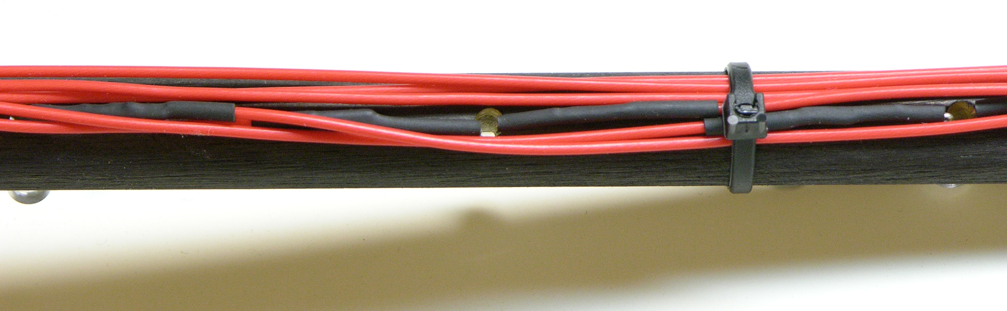
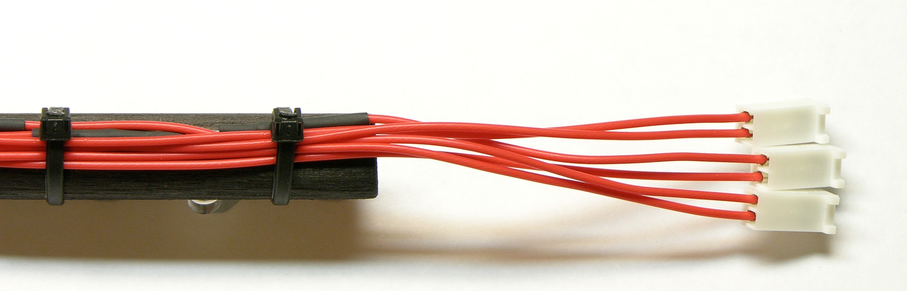
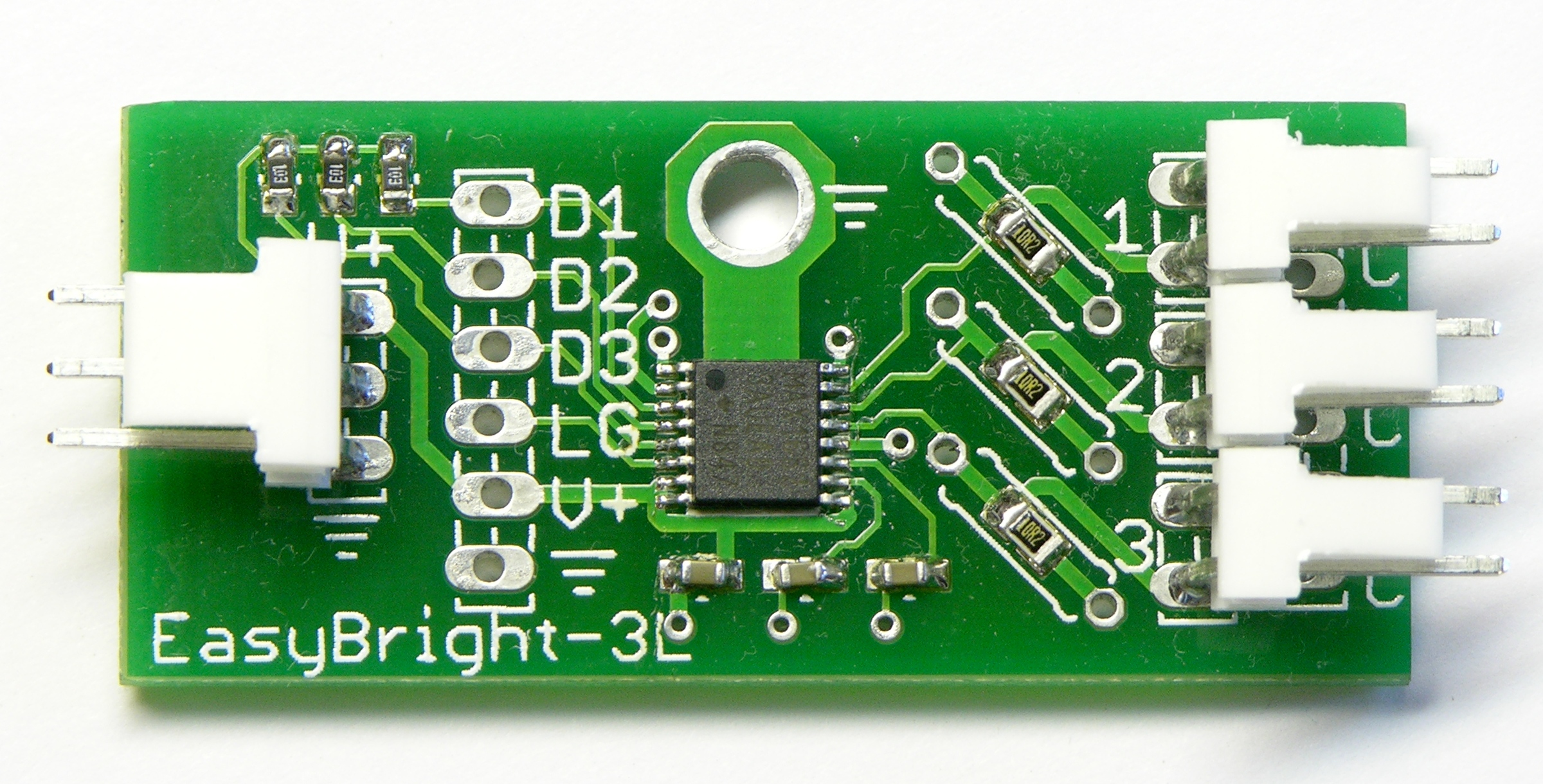
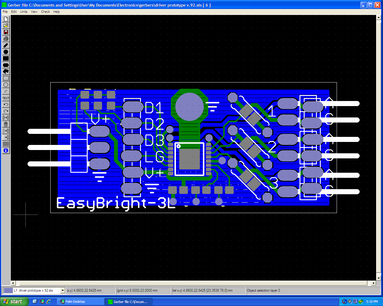
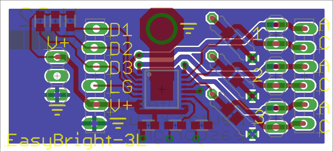
I’ve worked around the lack of plated through holes by laying out boards that don’t require them, always carrying a signal from top to bottom using a component lead that can be soldered on both sides. But this means no vias (soldering pins top and bottom just to change layers is a pain) and only crossing layers at resistors and diodes. It means always routing connections to electrolytic capacitors on the bottom, ’cause you can’t get to the top side of the board to solder unless you stand the capacitors way up on their leads. It means routing traces to headers only on the bottom, or sliding the plastic guide up on the pins to solder the top side and then sliding it back down. It means a dozen little design compromises for a prototype board that don’t need to be made for a board I’m going to have commercially manufactured later. It means not only extra effort to accommodate my prototyping methods but also extra effort to undo that work before going to manufacturing.

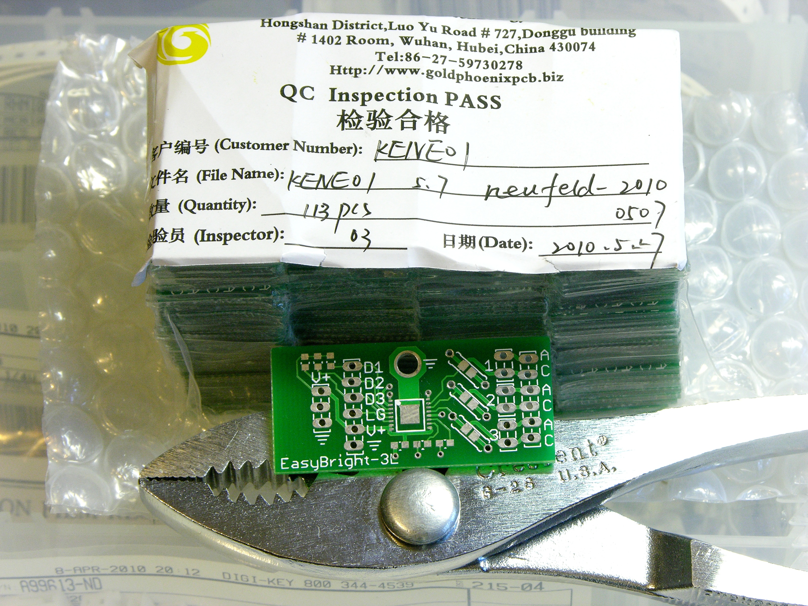
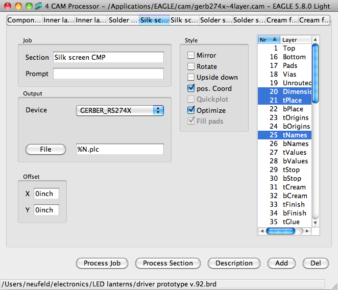
SparkFun Electronics created BatchPCB as an offshoot of their own PCB prototyping contract. They aggregate orders from multiple users, tile them together onto standard-sized panels, upload the panels to Gold Phoenix, get the boards manufactured, receive the shipment from Gold Phoenix, sort out the boards, and send them back. They charge $2.50 per square inch, which is higher than you’d pay if you were ordering 100 square inches — but far less than you can pay anywhere else if you only want a few square inches of prototype. And they charge a flat $10 handling fee per order, regardless of how many designs you include in your order.

They suggest it’ll take about three weeks to get your order. My experience has been two weeks. It sounds like a long wait, but as they say:

As we develop projects, we always get at least one PCB design onto the week’s batch panel. While one design is being fabbed, we have new PCBs for another design already arriving from a previous batch – we always have new PCBs to play with!

My Summer with BatchPCB

I’m trying to place an order every two weeks and to order boards for multiple projects each time. I’ve received two batches so far and I submitted a third this weekend.

Circuit boards from BatchPCB

I’ll say more about these designs as I work on the projects, but starting at the top and progressing in reading order:

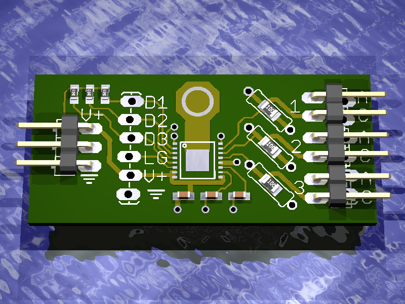
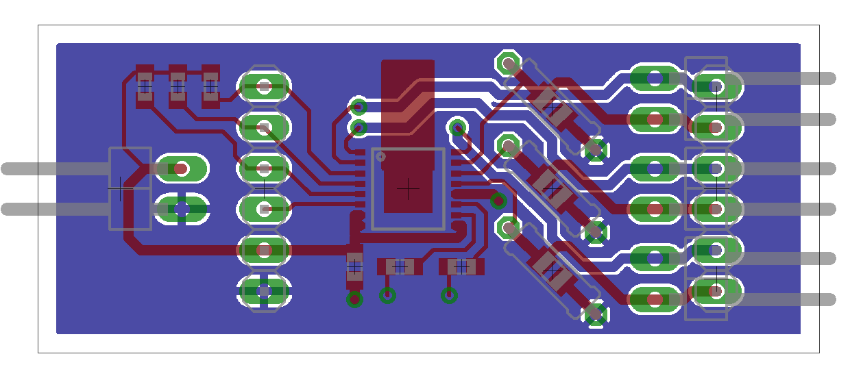
  • Logic gate boards to help bridge the huge gap between what happens in the digital design lecture and lab. My classmates with no prior experience did not gain much academic value from poking opaque ICs into breadboards.
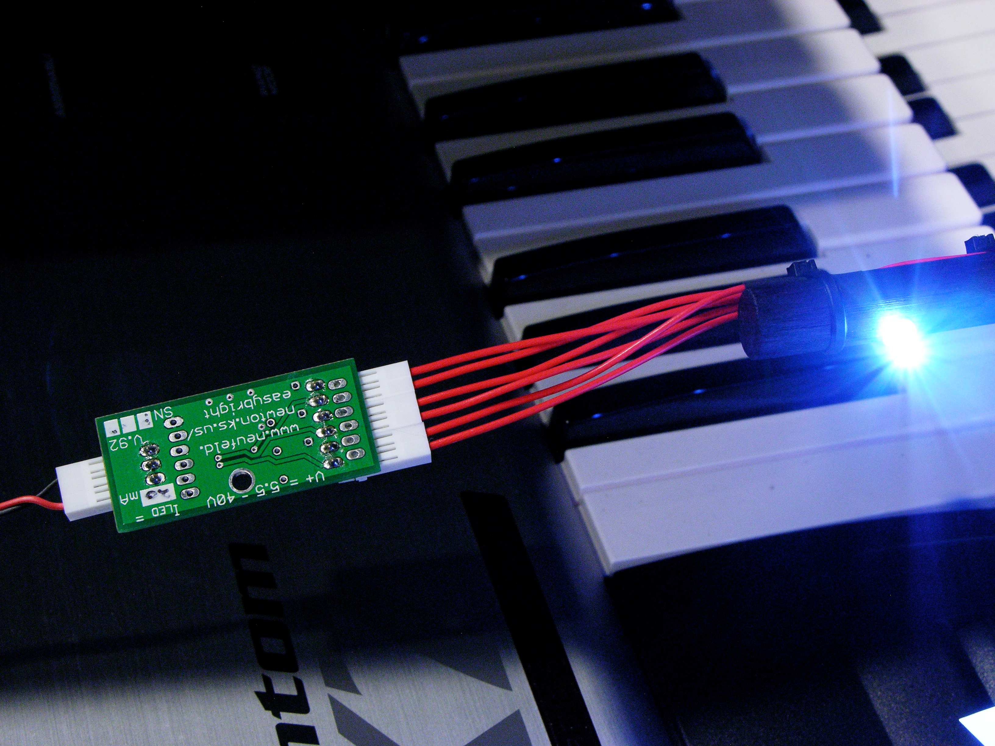
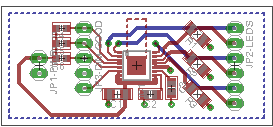
  • A Freeduino-derived board for my personal use, manufactured as a proof-of-concept that I have the right components and schematic to embed an Arduino-compatible core into projects of my own. (I will of course publish all source files for designs that I distribute to anyone other than myself.)
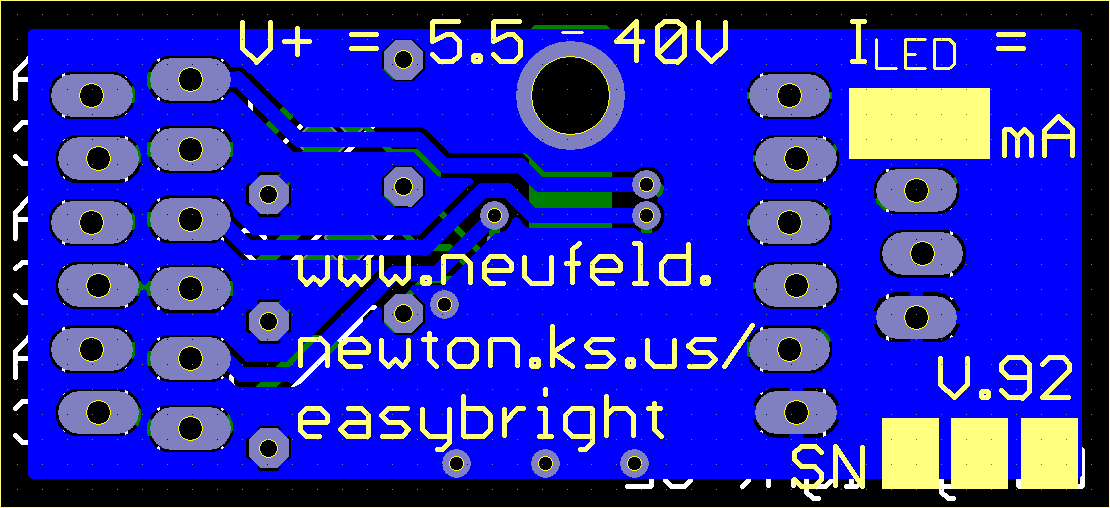
  • The first half of a pair of boards to breakout a headphone cable and jack for breadboarding, to plug an iPod’s headphone output into op-amp filter circuits and listen to the results.
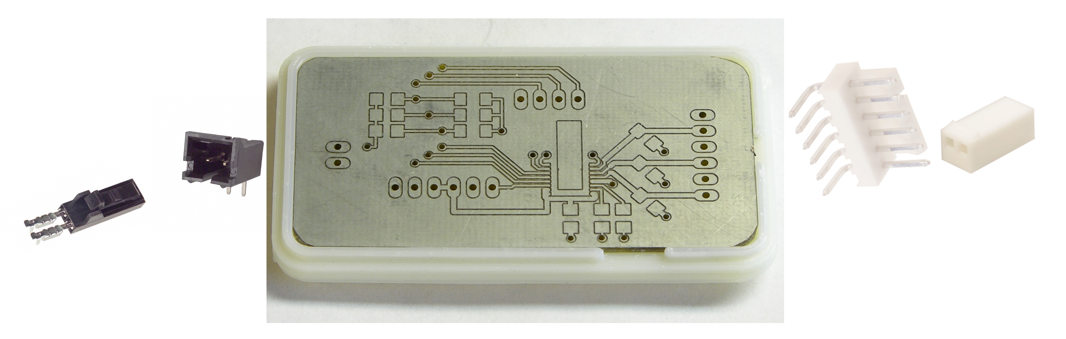
  • A board for testing component lead fit against through-hole sizes. To date, I’ve used calipers for measuring lead sizes for PCB design. I’m curious whether testing against a physical board gives me any different expenditure of time or quality of results.

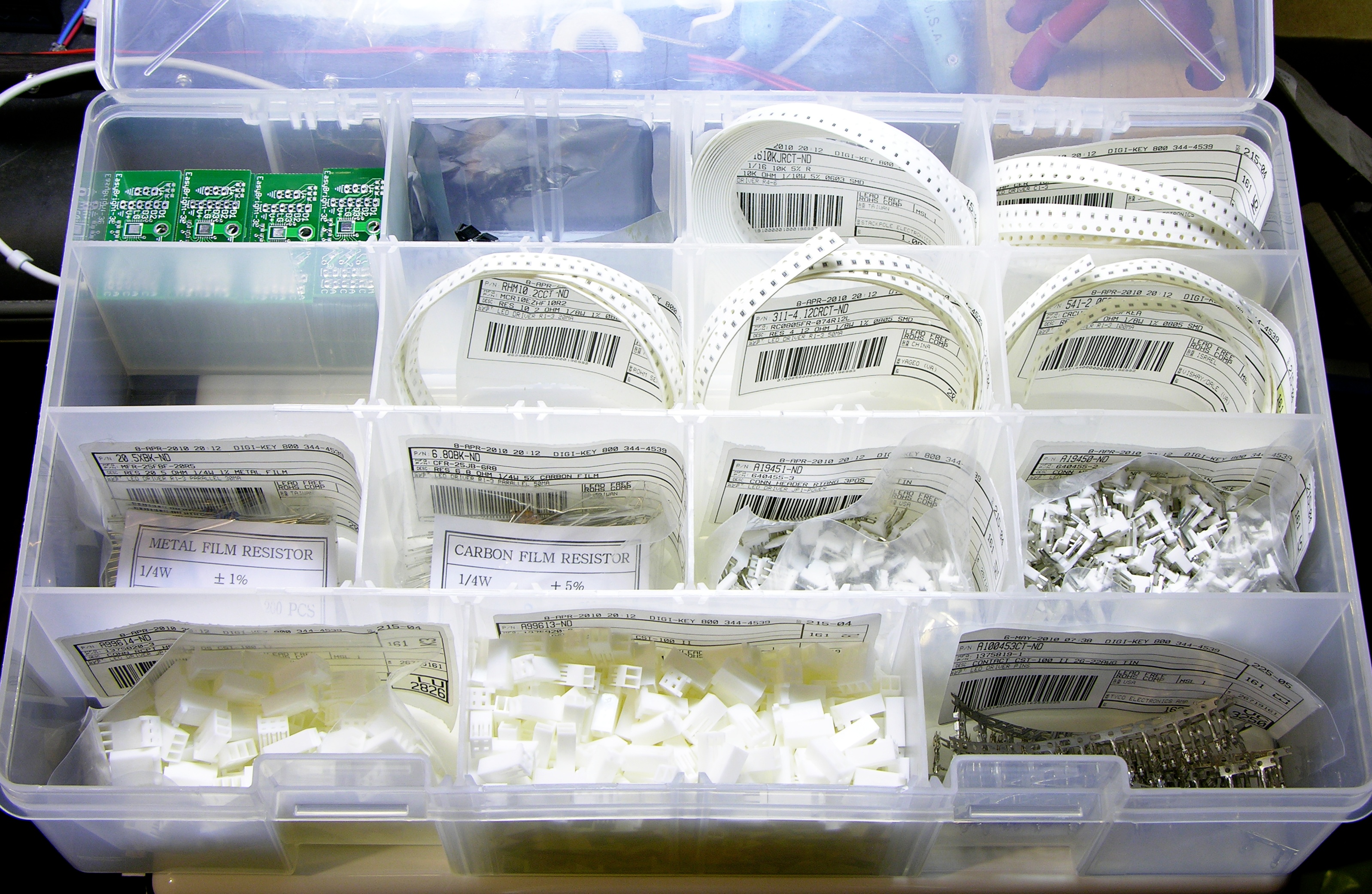
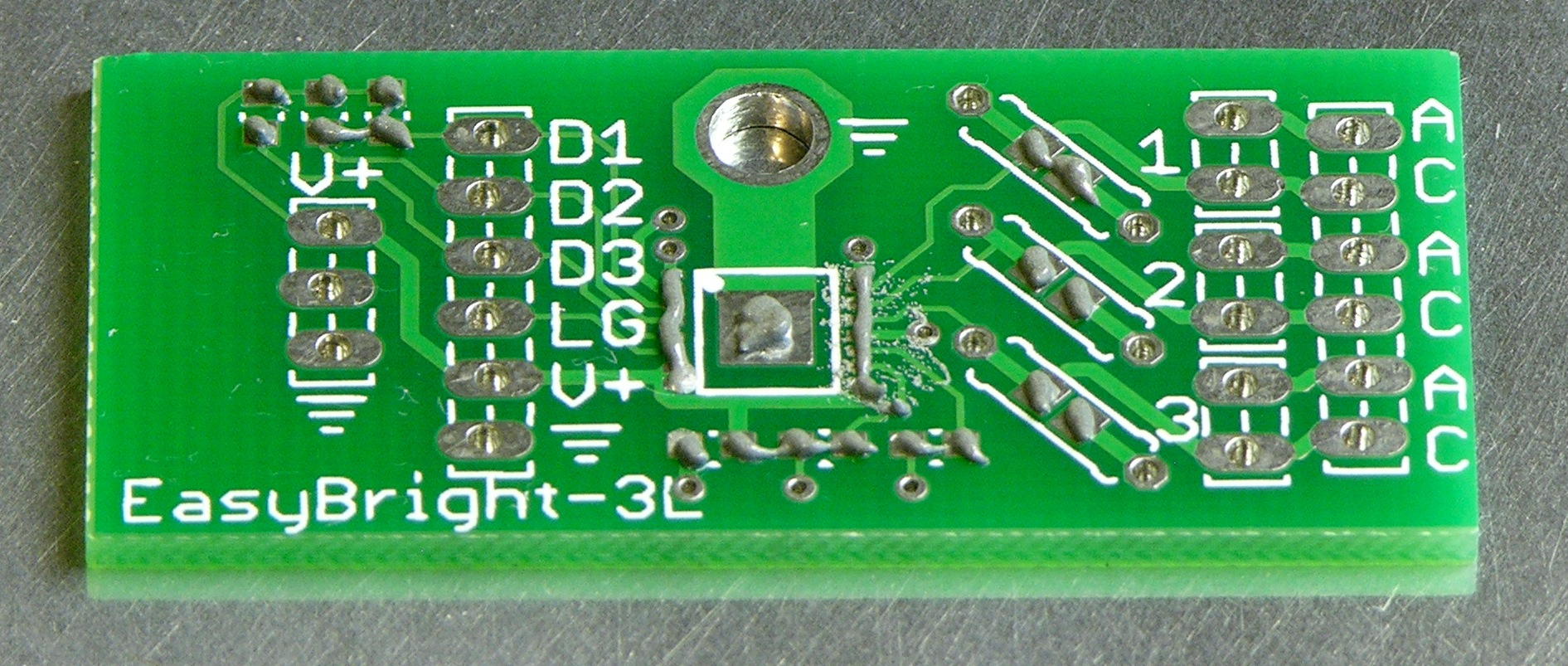
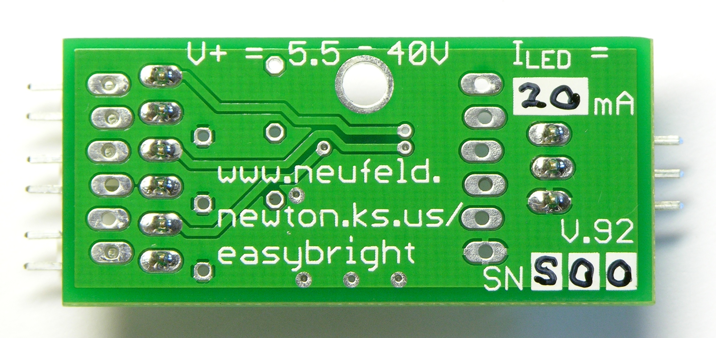
The logic gate boards were my first batch. I ordered four each of two variants of the boards, assembled a few, and discovered that I don’t like soldering 0603 SMT as much as I thought I did; so if I make more, I’ll be changing the boards to use 0805 components.

Lesson learned: Order only one of your first prototype, regardless of how sure you think you are that you’ve finalized the design.

So why so many of the other boards? I did order only one of each … but SparkFun, bless their hearts, appears to fill wasted space in each panel with small customer boards that they give back to their customers as a bonus; and I happened to have small designs in this batch.

Transistor-Based Variable Current Drive for LED Calculator

Monday, September 6th, 2010

I’ve put off working on my LED calculator project for far too long, at first trying to find the right handheld case to put it in and then later hoping to be able to manufacture a case myself. I’m not having any luck with that right now and if I keep waiting I’ll wait forever; so I’m resurrecting the project with the intention of selling it as a kit sans case.

The idea is to expand on a simple LED tester by allowing the user to plug in an LED, dial in the LED brightness, and then read information on an LCD showing the LED voltage drop, the current current, and the value of current-limiting resistor to use in a target circuit.

A microcontroller determines this information by measuring the voltage drop across a series current-sense resistor to calculate the current and measuring the voltage drop across the LED to calculate how much voltage will drop across the current-limiting resistor in the target circuit and what that resistor value should be.

Variable Resistor Drive

LED calculator drive circuit

Until now, all of my prototyping has used a variable resistor in series with the LED to set the current. After subtracting the LED’s forward voltage drop from the supply voltage, the variable resistor dominates the resistance of the remaining series chain (which includes the current-sense resistor), thereby setting the series current.

LED calculator prototype with direct potentiometer drive

This does give control over the LED current and brightness, but the problems with this method are:

  • A small-valued potentiometer doesn’t provide enough resistance to dial down to low enough LED currents. For example, a 1K pot with the circuit running on 9V won’t deliver less than 6mA, depending on the LED color (and voltage drop); and modern, high-efficiency LEDs are surprisingly bright at 6mA.
  • A large-valued potentiometer has an extremely non-linear current response, with all the “action” at the very end of its rotation.

Here’s the response of two different LEDs with a 10K potentiometer:

Position Green LED Current Blue LED Current
0 1mA 1mA
1 1mA 1mA
2 1mA 1mA
3 1mA 1mA
4 1mA 1mA
5 2mA 2mA
6 3mA 2mA
7 4mA 3mA
8 5mA 6mA
9 34mA 21mA
10 100mA 89mA

Very slow response until near the end of the potentiometer’s rotation, at which point the response is so rapid that it’s very difficult to control
And of course this makes sense, as it’s the hyperbolic curve of I = V/R.

Transistor Drive

Last week I started looking at improving the range and linearity of the LED current. I’m not looking for a perfectly flat response curve nor for a true constant-current drive; I just want a somewhat better response. What came to mind was this simple PNP transistor circuit — actually an even simpler version without R1 and R3, but I’ll explain their purposes in a bit.

Transistor LED current control circuit

The theory is that R2 (or R1 + R2 + R3) acts as a voltage divider across the power supply, linearly setting a drive voltage. R4 (nearly) linearly turns this voltage into a current sink across the PNP transistor’s emitter-base junction; and because R4 >> R2, R2 presents a “stiff” voltage source to R4, meaning we can largely ignore R4′s effects on the voltage division.

Thus R2 provides (nearly) linear control of the emitter-base current. In the common-emitter configuration, the PNP transistor amplifies the current by the transistor’s β (about 150-200 for a small, general-purpose PNP like the 3906) for a correspondingly higher emitter-collector current

IEC = β IEB

which goes through the LED and the sense resistor, providing (nearly) linear control of the LED brightness by turning R2.

Well, that’s the theory, anyway. This weekend I dug out the prototype and built up the transistor control to test it in practice.

LED calculator prototype with transistor current drive

(70s decor courtesy Radio Shack.)

The first thing I noticed was a section at the CCW end of R2′s travel in which nothing happened, because R2 wasn’t providing more than the transistor’s cut-in voltage — that is, although VB was less than VE, it wasn’t enough less to overcome to emitter-base forward voltage drop and bias the transistor down into the active region.

I tried installing a small-signal diode “above” the potentiometer so that VB would always be at least .6V below VE and eliminate R2′s dead region, but the diode’s forward voltage drop was a little too high (it did too good a job) and the resulting minimum LED current was a little higher than I liked. I settled on adding R3 in that position, selecting 68Ω as a value that worked well with both traditional and high-power / high-efficiency LEDs and with both 9V and 7.2V supplies.

With a 9V supply and R3 = 68Ω, I tried three different values of the base resistor R4.

R2 Position R4 = 10kΩ R4 = 22kΩ R4 = 47kΩ
Green Blue Green Blue Green Blue
7:00 0mA 0mA 0mA 0mA 0mA 0mA
8:00 0mA 0mA 0mA 0mA 0mA 0mA
9:00 8mA 7mA 3mA 2mA 1mA 1mA
10:00 30mA 30mA 15mA 13mA 7mA 6mA
11:00 46mA 42mA 24mA 22mA 13mA 11mA
12:00 56mA 47mA 34mA 32mA 17mA 17mA
1:00 60mA 48mA 42mA 40mA 24mA 22mA
2:00 62mA 49mA 49mA 44mA 29mA 26mA
3:00 62mA 49mA 53mA 46mA 32mA 30mA
4:00 63mA 49mA 55mA 47mA 34mA 31mA
5:00 63mA 49mA 55mA 47mA 34mA 32mA

The table shows a similar effect at the other end of R2′s travel in which the LED current was pretty well maxed out and not increasing any further. I think I was hitting the knee between the transistor’s linear region and saturation, meaning increasing IEB was no longer increasing IEC. Experimentation gave me R1 of 200Ω keeps the transistor pretty well out of saturation and gives a satisfyingly more-linear response than what I measured here.

The 0mA readings at the beginning of the table, by the way, are a bit deceptive — some of my test LEDs are actually lit in that region. I’ve updated the Arduino code to show tenths of a milliamp when the reading is below 10mA, and I can see LEDs glowing with as little as .1mA. Probably not a value of interest for most people, but it could be effective for making flickering gas lamps for model railroads.

Choosing Values

R4 = 22kΩ looks like a pretty good compromise between providing a near-linear response and covering the range of LED currents I expect most people would be interested in testing, so I’ve tentatively settled on it.

I’m still fiddling with values to give good performance at both 9V (alkaline battery) and 7.2V (NiMH), because I use rechargeables almost exclusively and want to make this work well on rechargeables to encourage other people to do the same. The problem is,

Vsupply = 7.2V
VEC ≈ .8V
Vblue LED ≈ 3.5V

VR5 = Vsupply – VEC – VLED = 7.2V – .8V – 3.5V = 2.9V

ILED = IR5 = VR5 / R5 = 2.9V / 100Ω = 29mA

In other words, running on a 7.2V battery, with the transistor saturated, a blue LED with a 3.5V forward drop maxes out at 29mA; and it gets worse with a battery that’s not straight out of the charger and some white LEDs with a higher forward voltage drop. I’d like to enable people to test up to 50mA, to cover high-brightness LEDs, so I’d like to push this maximum current a little higher.

R5 = 68Ω gives ILED up to about 42mA, which isn’t as high as I like; but the tradeoff is that a smaller R5 gives me a smaller voltage range to sample in the A/D converter, hence lower resolution for the display. 68Ω seems like a good compromise. And I’m already thinking about a DPDT switch to change the resistor and alert the microcontroller about battery chemistry.

EasyBright on Stage

Tuesday, May 25th, 2010

Music stand wand light with lens flare

Saturday night the EasyBright already got its public debut! I played a pair of classic rock concerts Friday and Saturday nights, and Friday had trouble seeing my music (occasionally folded out to four pages) with the clip-on stand light I was using. Saturday after assembling the EasyBright, I built an LED “wand” music stand light that worked marvelously.

End of LED wand music stand light

I didn’t have a lot of time for construction, so I cut a 1/2″ dowel to 3′ length and drilled eighteen 1/8″ holes through it (axially, not longitudinally) every 2″. Paint wouldn’t dry before the show, so I sanded the dowel and then colored it with a permanent marker. I then installed bright flat-top LEDs with a good viewing angle into the holes and bent the leads out in opposite directions.

Wiring on LED wand music stand light

I lap-soldered teflon-insulated (heat-resistant) wire from LED to LED with heat-shrink tubing preinstalled — but didn’t shrink the tubing until after I had tested the LEDs, in case I needed to repair any solder joints. I skipped LEDs to make an A-B-C-A-B-C pattern so if a chain failed, I’d lose light evenly along the whole wand instead of all in one section.

Connectors at end of LED wand music stand light

I crimped connectors onto the wires, connected everything to the EasyBright, put an appropriate connector on a 24VDC wall wart, and fired it up perfectly on the first try. (Such luck!) I disconnected the wand, reseated and shrank the heat-shrink, zip-tied the wires in place, and then powered up the wand to burn in for an hour before leaving home for the concert.

LED wand music stand light

On stage, it delivered a very even wash of illumination across my music, giving me a great view all through the show.

EasyBright circuit board driving LED wand music stand light

The circuit board is so lightweight, it was comfortably suspended in mid-air between the keyboard rack and my music stand by the power and LED wires. For the long term, I’m trying to decide whether how it should be mounted to the wand — perhaps attached near the end inside a sleeve of giant heat-shrink.

Assembling the first EasyBright

Tuesday, May 25th, 2010

EasyBright components

Last week while watching Mannequin (a very young and fresh Kim Cattrall, a goofy plot, and music by Starship — what could be better? okay, if it had John Cusack and were set in Shermer, Illinois, yes, that would be better) I split all the EasyBright components into a parts bin for easy access and portability.

Saturday afternoon I put together the first sample.

EasyBright-3L constant-current LED string driver PCB with solder paste

This is waaaaaay too much solder paste for 0603 parts and 1/40″ IC pin spacing. I had to remove several solder bridges from the IC, and the passives had solder mounds instead of fillets. I took the picture specifically to record how much paste I used so I could adjust on the second attempt.

EasyBright-3L constant-current LED string driver, front

Here’s the cleaned-up board, front side.

EasyBright-3L constant-current LED string driver, back

Back side, with hand-written labels for the current rating and the serial number (S00). The “permanent” marker comes off easily with rubbing alcohol — I need to get some clear nail polish to seal it in.

Changes

Even before assembly, I had made notes about (and started implementing) things to fix whenever I print the next boards:

  • Change the IC’s ground connection from a via outside the IC footprint to a trace going straight in to the heatsink pad. I had routed that connection before I confirmed with Maxim that the pad is okay to connect to ground — it’s just not okay to be the only ground — and then forgot to go back and change it. Removing that via gives me a little more room to route the bottom-side LED power traces cleanly, and also:
  • Increase the pad size on the optional through-hole current-sense resistors. This, believe it or not, is EAGLE’s default pad size, and I think it’d be challenging to solder without a good, narrow-tipped iron.
  • Increase the trace isolation on the solder-side ground pour. There’s no reason to have it that close to the pads.
  • More subtle, I spaced the 2-pin connector pads an extra .02″ apart to see whether I could get the connectors to friction-fit for ease while soldering. They don’t quite. Either change the library footprint to space the pads a little further apart or just get used to pinching the leads together before stuffing the parts and soldering, which works better than I had expected.

I’m still delighted!

Gold Phoenix for EasyBright PCB Manufacturing

Monday, May 24th, 2010

Two and a half weeks ago, I finished up the CAM files for my first set of EasyBright LED driver PC boards and sent them off to have boards made.

PC board order from Gold Phoenix

While shopping around for board houses, I had narrowed my choices to two. Here’s how I made the final selection of Gold Phoenix — not, as it turns out, whom I thought at first I was going to pick.

(more…)

Viewing PCB Gerber Files Before Manufacturing

Thursday, May 6th, 2010

I’ve spent my last week and a half’s free time going back and forth among EAGLE, eagle3d, 1:1 printouts, and the Viewplot Gerber viewer. That’s how long it took me to get the silkscreen layer tweaked to my satisfaction — which I completely didn’t anticipate.

Thank you, thank you, thank you SparkFun for emphasizing how important it is to view your Gerbers before submitting (search in page for “Something I highly recommend”).

eagle3d view of LED driver prototype

I had already rendered the board layout in eagle3d (pay no mind to the test holes I used to figure out that eagle3d doesn’t make holes through copper that’s part of a polygon, which its documentation clearly states if you bother to read it) and thought it looked pretty good.

But I followed Nate’s advice, installed Viewplot, and was rather startled to see what my board was really going to look like.

Viewplot Gerber view of LED driver prototype

The silkscreened boxes for the plastic “keepers” on the pin headers are fairly faithful to the connectors I’m using, but what’s with putting the pins in the silkscreen? I don’t need a shadow of the pins on the board.

Also the 0805 SMT resistors and capacitors don’t have silk around them showing which pads belong to the same component. It’s easy enough to figure out on this small board, but I’d like to develop good habits.

EAGLE CAM processor showing layers going into top-side silkscreen

EAGLE’s CAM processor lets you pick which PCB layers are used to generate each Gerber file, and there’s not much in my top silk layer. The pins must be in tPlace, so I used the PCB layout editor to preview what would happen if I turned it off …

EAGLE PCB layout with tPlace layer switched off

I lost the header outlines as well as the pins, as well as the outlines for the optional through-hole resistors. That’s not gonna work.

Changing package of two-pin connector in EAGLE PCB layout

Exercising outrageous optimism, I tried changing my header packages from right-angle to vertical, hoping they’d have more appropriate package outlines (still in the tPlace layer).

EAGLE PCB layout with header type switched, tDocu on

Better — no stray pins in the silkscreen. Now guardedly optimistic.

EAGLE PCB layout with tDocu off and supplemental silk drawn in tPlace layer

I turned off the tDocu layer that shows the physical outlines of components, and which isn’t (and mustn’t be) included in the silkscreen Gerber because it would interfere with soldering, then added lines in tPlace to indicate the edges of SMT components.

Silly me — I thought I was done!

Viewplot Gerber view of revised LED driver prototype

Back in Viewplot, look at how the silkscreen around the power connector is now crowding the pin labels. Aaargh! There’s not room to move them far enough away.

Viewplot Gerber view of revised LED driver silkscreen

I went back to my connector library and designed two- and three-pin versions of “locking” connectors based on the SparkFun locking connector concept. (See footnote about SparkFun EAGLE library license terms.)

The Gerber view looked pretty good now, except the ground symbol was too close to the power header and a little visually confusing.

Viewplot Gerber view of LED driver with working drill holes

I moved that down a bit and in my next trip to Viewplot discovered how to get the drill holes to show up: don’t load the drill rack file into Viewplot, just the drill file itself. Getting visualization with holes and confirmation that there’s really a mounting hole through the heatsink — outstanding!

Somewhere around this time I also printed out the solder-side of the board to make sure that the boxes I made to write in (visible in the next screen shot) were large enough for me to write in. They weren’t. I enlarged them.

Done now, maybe?

Viewplot Gerber view of LED driver with working drill holes, back

Oof, look at all the problems with the silkscreen on the back side. The top line looks like I’m incrementing V by 5.5-40V (C joke), and if I fix that I need to move ILED‘s = further away also. The / in the URL is awfully close to the solder pad, and the box for me to write the “factory”-configured LED current could stand to extend a little closer to the “mA” label.

Props to Nate at SparkFun again (search in page for “Label everything, all the time”) for reminding me to put the input voltage range and output current rating on the board, BTW.

Viewplot Gerber view of final LED driver design, back

Fixed! Really! Done! If I stare at this thing any longer, I’m going to start hand-kerning the vector font.

I zipped the files and uploaded them to Gold Phoenix last night.


SparkFun EAGLE Library License Terms

I’m not using SparkFun’s EAGLE library nor a derivative of their library file because I haven’t got a response from them whether their cc-by-sa license is intended to be:

  • like the GPL, meaning that if you use their library in your board design you have to open-source your whole design — which I will do after I’m confident the design is right but not immediately upon shipping — or
  • like the LGPL and you can use the library in your product without open-sourcing your design but you would have to open-source derivatives of the library itself.

So my connector library is most definitely based on Pete Lewis’s idea to skew pin positioning from side to side to make a header friction-fit in a board for soldering, but (as far as I know) the idea is not patented and I’m in the clear. My library is a reimplementation from scratch of the idea, so is not derivative of their library.

I hate playing games like this and I would love to toss my library and use SparkFun’s if I can get a verdict from them on the licensing. Also as soon as I’ve got boards tested and working and I’m ready to publish the design files, I can switch back to their library too.

Update 07-May-2010: I heard back from SparkFun and it will be fine for me to use their library. I’ll look at switching back on the next iteration of the board.

Names for LED Driver

Wednesday, April 21st, 2010

The LED driver board is nearing its final configuration (I need to convince EAGLE that the mounting hole has a hole in it; and don’t worry, those aren’t really the headers I’m using) and I’m about ready to send it off to be manufactured. But I’d really like to come up with a great name for it, to have silkscreened on the back side.

Rendering of LED driver PC board

I’d like something whimsical but which still relates to its function as an LED driver. Fun hobby electronics names I love: Adafruit, MintyBoost, BlinkM, SparkFun, MakerBot, and CupCake.

I’ve considered Illumerator, Illumifier, and variations Lumerator and Lumifier (which is probably TM and a bad idea). Whatever I settle on will have -3L appended, to distinguish this 3-string linear driver model from the -1S switching model I want to do next.

So I welcome suggestions for great names. I’ll be happy to send you a couple of drivers if you’re the first person to suggest something I end up using.

Warning: I don’t care for variations of my name that feel like they came from the “makin’ copies” sketch.

What LED Currents Should I Offer?

Saturday, March 27th, 2010

The MAX16823 that my LED driver is built around uses current-sense resistors to set the LED strings current to .203V / R.

So for the maximum 100mA, R = 2.03Ω; for 20mA, R = 10.15Ω.

PC board layout for LED driver

I’ve laid out the board to accommodate both SMT and through-hole sense resistors. I’d like to offer boards preassembled for at least 100mA and 20mA and boards without sense resistors so you can provide your own resistors for custom currents.

Should I offer other preconfigured currents besides 100mA and 20mA? Do I need to bother with 15mA?

Let me know in the comments what currents you’d like to have. Just because you ask for something doesn’t mean I’ll provide it; but if enough ask for the same thing, I very well might.

Opinions Wanted: Connectors for LED Driver

Saturday, March 20th, 2010

The long-languishing linear LED lighter is back in my “get it done” pool. I have the parts sourced, the design refined, and a big bag of utterly failed attempts to print an acceptable case for it on my CupCake. Fine. Forget the case. No case.

The project, to refresh your memory, is a linear driver for three strings of LEDs, up to 40V and 100mA per string. You supply your own power (5-40VDC), LEDs, and wire.

After spending two hours looking through 250 pages of connectors in the Digi-Key online catalog (I am not kidding), I’m distressed to discover that the least expensive connectors I can find are going to cost about $2 per board. Feh! But I want the power and LED connectors to be polarized, and that’s more expensive than plain ol’ .1″ headers.

LED driver board and connectors

Here’s a mockup (clickable for the big pic, like all the photos here) of an early prototype PCB with product photos of the connectors I’m leaning toward. On the right, a six-pin header for three LED strings and a representative two-pin plug that’s polarized by virtue of the semi-latching bump. On the left, a two-pin header for power and definitely-latching matching plug.

Note that the male connectors are on the board to reduce the opportunity for shorting what’s on the ends of the wires while they’re unplugged and flailing around.

Questions:

  1. Is it reasonable to expect people to plug three two-pin connectors into the right places in a six-pin header?
  2. Is it worth making the power connector different from the LED connectors, to make it harder to misconnect things?
  3. How many people are going to crimp pins onto the wrong wires and have to start over?

Opinions in the comments, please.

If you think you can find me less-expensive polarized connectors with .1″ spacing (I want to offer the driver with straight male headers for breadboard friendliness) that I can buy from a supplier as reputable as Digi-Key, please provide direct links to at least the header and ideally the plug and crimp pins. Free LED driver if you actually come up with something I like better.


Addenda 21-Mar-2010

Thanks for the responses so far! A few additional notes:

Connector Cost

The connectors I show above come to about $2 total per board, not $2 each. That’s still a larger fraction of the electronics cost than I’m happy about.

Connector Size and PCB Size

The current iteration of the board layout is much smaller than that shown above:

LED driver board layout

I’m trying to make it as small as possible (A) on principle, (B) to save on board manufacturing cost, and (C) to make it easy to “hide” the driver within whatever you’re building. I have a little more optimization to do; but you can see that the board size will very soon be determined by the size of the connectors.

Because of this, I would really rather not leave extra “key” pins in the LED string connector — they’d widen the board. (Arguably I could then shorten it, but I’m not convinced I could really make that happen, given the distance I need to fan traces out from the TSSOP. The TQFN pinout doesn’t make things significantly better, either.) I’d also rather not use connectors with “walls” between the two-pin pieces, as they’d increase the PCB width (height?) by at least .2″.

Also if I go with the six-pin connector idea, the female headers need to have thin outer walls so they can fit side-by-side between adjacent pins.

LEDs and 6-Pin Connector

By my read of the MAX16823 datasheet, if you misplug an LED string one pin off, it simply won’t light, nondestructive to both the LED and the string. I assume you would then look at the plug and see you had misplugged it and replug it correctly — so this should not be a catastrophic event.

I also intend to indicate the correct divisions of the 6-pin connector in silkscreen.

I know people will still get it wrong occasionally, but since it won’t hurt anything — good enough?


Addendum Noon 21-Mar-2010

Asmodeus has found the connectors I want to use and pointed out the (obvious) way to space them to meet my board criteria.

If I need further input, I’ll mock up another picture with the latest plan and start a new post. Thanks to you all, and comments are now closed!