Archive for June, 2007

Driving a Bicolor LED from a Single Output Pin

Saturday, June 30th, 2007

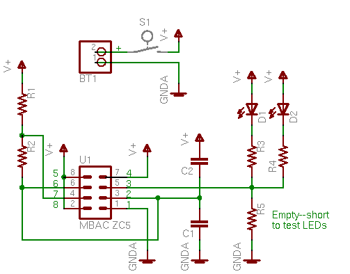
I’m working on a control system for my stereo, with more information on that project to be posted soon. I was running into a problem having enough pins on my PIC to connect all the inputs, pushbuttons, LEDs, and outputs.

Yesterday I was talking to Tom and describing how each bicolor output LED requires two microcontroller pins to control both colors. I’m sure this scheme has been used a million times before, and I may even have seen it before, but I was very pleased to realize in a flash of insight how to drive a bicolor LED from a single output pin.

Driving a bicolor LED from a single microcontroller pin

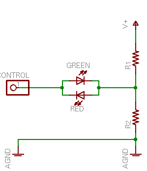
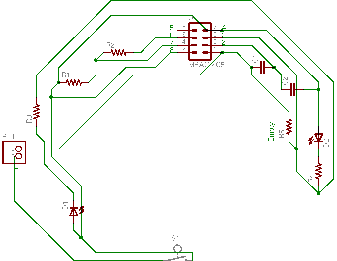
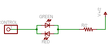
Instead of connecting the LED between the control pin and V+ or ground, connect it to a voltage divider between the two. Raise the control voltage to V+ and the green LED will conduct through R2. Lower the control voltage to 0V and the red LED will conduct through R1. Here’s the best part — change the control pin to an input and it’ll go into a tristate (high-impedance) mode, leaving the left end of the bicolor LED floating, with both elements off. Perfect! That saves my project!

I breadboarded this circuit with 330Ω resistors, and the LED was quite a bit dimmer than normal. Well, of course it was; it’s running off less voltage than usual. Plus the voltage divider isn’t exactly a stiff current source. But I was curious exactly how much less voltage (seems obvious, but wouldn’t it be nice to know for sure?), and what was the exact series resistance (ah, somewhat less obvious, eh?).

Thévenin Analysis

Thévenin’s Theorem states that any linear circuit (comprising only voltage sources and resistors) can be represented as a single voltage source and a single series resistor, and provides a very simple method to determine the equivalent voltage and resistance. So a Thévenin analysis of the voltage divider will give us a simpler model of that section of the circuit, which can then be used to determine the actual LED current.

First, to determine the Thévenin voltage (VTH), mentally remove the load from the circuit and use Kirchhoff’s Law to find the voltage at the load connection.

Determining Thévenin equivalent voltage

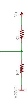
In this case, assuming R1 = R2, VTH is V+ / 2.

Next, to determine the Thévenin resistance (RTH), (mentally) short out all the voltage sources and use Kirchhoff to find the overall resistance looking into the circuit.

Determining Thévenin equivalent resistance

In this case, mentally shorting V+ to ground puts R1 and R2 in parallel, giving

RTH = (R1 * R2) / (R1 + R2)

Or again in the case where R1 = R2,

RTH = R2 / 2R = R / 2

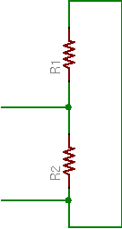
Thévenin Equivalent Circuit

So assuming R1 = R2, the voltage divider is equivalent to a voltage source of V+ / 2 in series with a resistance of R / 2, which gives this simplified circuit:

Bicolor LED drive circuit with Thévenin equivalent voltage divider

This makes it easy to determine the LED current (ID). Whether the control voltage is at V+ or 0V, the LED and Thévenin resistor will see a voltage of V+ / 2 (forward or reverse).

Using the zeroeth approximation of a diode as a device that conducts electricity in a forward direction with no voltage drop, the resistor has the full voltage across it, so the resistor current

IR = (V+ / 2) / (R / 2) = V / R

and ID = IR. For a 5V supply and 330Ω resistors, I = 5V / 330Ω ≈ 15mA.

But that’s exactly the same current (and concomitant LED brightness) we’d expect running an LED from a full V+ with a full R, and I distinctly noted that the LED was dimmer. What’s going on?

LED Voltage Drop

The answer lies in the first approximation of an LED as a device that conducts electricity in the forward direction with a voltage drop and no resistance. The bicolor LED I was using has about a 2V drop in either direction (about 2.08V green and 1.95V red, at the temperature and moment I measured).

Still using a 5V supply and 330Ω resistors, an LED voltage drop VD = 2V gives a voltage across the resistor of

VR = (V / 2) – 2V = 2.5V – 2V = .5V
IR = VR / RTH = .5V / 165Ω ≈ 3mA
ID = IR3mA

Whoa! That’s a whole different story! Halving the effective supply voltage dramatically exaggerates the effect of the LED’s voltage drop.

In fact, to get back up to ID = 15mA:

RTH = VR / IR = .5V / 15mA &symp; 33Ω

That’s an order of magnitude lower current-limiting resistance to get the same LED current and brightness.

Even worse, note that this circuit (the original) has a continual current of V+ / 2R through the voltage divider. With 330Ω resistors, that’s 7.6mA (38mW), which may be tolerable in a non-battery-driven circuit; but with 33Ω resistors, that’s an unacceptable 76mA (380mW) per LED driver!

Tolerable Adaptations

So how can we make this circuit work well enough to be practical? Here are a couple of options.

First, note that the current-limiting resistance needed to be made so low because half the supply voltage is barely more than the diode’s voltage drop. With a higher supply voltage, more voltage would be “left” after taking out the LED’s drop, and a higher resistance could be used to get the same LED current.

But how far can we raise the supply voltage? For the circuit to work properly, the control voltage from the microcontroller needs to swing over the same range as the LED’s voltage divider. And alas, the PIC I’m using has a maximum VDD of 7.5V; or say a safe working voltage of 7V.

Adding 2V to V+ adds only 1V to the LED/resistor supply, increasing VR from .5V to 1.5V, or threefold. That translates into three times larger resistance and one third the voltage-divider power consumption — progress, but not as much as I’d like.

Second, note that the bicolor LED I’m using is not particularly high performance. Newer LEDs appear to me to be several orders of magnitude brighter at the same current. (Go check the amazing mCd claims of LED vendors on eBay. For the most part, they’re increasing efficiency, not current-handling capacity.) I’d gladly pay a little more for a much brighter LED that has lower current requirements for the same brightness.

Even one order of magnitude difference in LED efficiency pushes the voltage divider power consumption back into an acceptable level for the device I’m designing. It also cuts the power requirements for the PIC pin driving the LED. The datasheet quotes 25mA source or sink per pin, 200mA source or sink for all pins, but I’m old-fashioned and don’t want to push my luck.

One thing I don’t know is whether high-efficiency LEDs have the same voltage drop as traditional ones. With only 2.5V available for the LED, if higher efficiency comes at the expense of a higher voltage drop, I could “efficient” the circuit right out of its operating range.

Boosting the Drive Current

Before doing the actual calculations, I was pondering whether the PIC could really source and sink enough current to power all my LEDs as brightly as I want. I was musing out loud with Tom about how to build a transistor driver to buffer/boost the PIC’s output.

The driver needs to be a totem pole, meaning that it has two stacked elements so it can source the LED line up to V+ or sink it down to ground. The catch is the tristate trick that makes it possible to turn the bicolor LED off. Trying to cram a traditional complementary totem-pole output into this circuit IS WRONG AND DOESN’T WORK.

Bicolor LED circuit with incorrect totem-pole driver

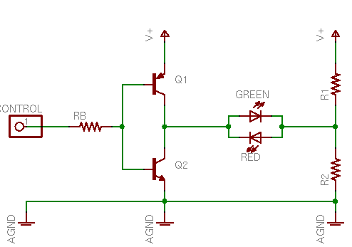
When the control line is high, the upper (PNP) transistor is off and the lower (NPN) is on, so the NPN pulls the driver output low. Likewise, a low control line pulls the driver output high.

The problem is when the control line is tristated. Then current flows through the PNP’s emitter and base to the NPN’s base and emitter, turning both transistors on and shorting V+ to ground. Real totem-pole drivers are designed to make sure this can never happen, even during transitions.

Here’s Tom’s solution, which like the tristate trick is probably a reinvention, but which is so clever that it still tickles me a day later to think about it.

Bicolor LED circuit with reversed totem-pole driver

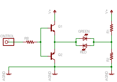
Just swap the NPN and PNP transistors in the totem pole, putting the NPN on top and the PNP on the bottom. When the control line goes high, the upper (NPN) transistor is on and the lower (PNP) off, so the NPN pulls the driver output high. Likewise, a low control line pulls the driver output low.

And a tristated control line leaves both transistors off and the driver output in a high-impedance state, because the emitters aren’t connected to the power rails to conduct through the bases any more.

Brilliant! Makes me want to use it, even though I realize with high-efficiency LEDs I no longer have any technical reason to. :-) But I’ll keep it in my bag of tricks.

Green Lines in My LCD Projector

Thursday, June 28th, 2007

I recently bought an ancient Sony “LCD Data Projector VPL-351Q” (video projector) on eBay for a reasonably modest price, without realizing just how ancient (and huge) it was. Fortunately, I was shopping geographically and was able to pick it up in person; it would have cost me a fortune to ship.

I’m interested in setting up a projector in the family room for watching movies, and this was a very affordable way to experiment before committing to an expensive course of action.

Sony LCD Data Projector VPL-351Q

That’s my 19″ stereo cabinet this thing is sitting on, with candlesticks elevating the front feet. It’s immense.

Old Lamp (Bulb)

Each time I power up the projector, it tells me that its lamp is old and needs to be replaced soon, which is no great surprise. (The onset of a lamp replacement warning seems to be a pretty strong motivator to retire projectors that are getting old anyway.) Of course, the few vendors I can find selling replacement lamps want $500 and up for them — a healthy order of magnitude more than I paid for the projector. Ha ha. This lamp is a bit dim, but not $500 dim.

I’m very curious how the projector knows the lamp is old — by counting hours of use (with a timer that I could reset?), or by monitoring lamp current. I’m also intrigued by the idea of rebuilding the lamp using something else — an automotive halogen bulb, perhaps. I assume I’d need to reuse the same reflector, and I think I might be able to manage it.

I’d also have to rig a different power supply for the replacement bulb — the original appears to run on 70V. The real problem would be if the projector monitors the bulb voltage or current (that I was no longer using) and shuts down if it seems improper. I’m not sure I’d be willing to go to the effort to rework or disable such a circuit.

Green Lines

Worse than the brightness, though, is a pair of green lines across the screen, just below the middle of the display. When I got it home and discovered them, I popped the case to have a look and found that the projector has a beam splitter, three monochrome LCD screens with color gels, and a beam . . . uh . . . unsplitter. So it’s plausible that the problem is isolated to the green LCD, and perhaps is nothing more than something is wrong with a row control line.

Image from my video projector with green lines

The black line, BTW, is a halogen torchiere — I’m temporarily projecting this onto the wall behind the couch. We’ll rearrange the furniture if it works out.

Inside the case, each LCD has two flex-PCB cables, presumably for row and column select. If the silk-screened labels are to be believed, the connectors in the upper center and right of the picture control the blue LCD, the lower center and left control green, and the one on the left plus the one disappearing off the upper left control red.

Sony VPL-351Q LCD control PCB

LCDs with which I’m familiar are clear when idle, and opaque when active. (Think of an LCD calculator or monochrome PDA — they’re grey when they’re off, not black.) If that’s how these LCDs work, then the bright green lines are rows that are letting green light through all the time — rows that are transparent all the time — rows that are never getting activated. Maybe I just had a bad connection on a pin or two.

(The connectors don’t have nearly as many pins as the horizontal and vertical resolution of the LCD, so my hypothesis isn’t perfect. A one-to-one match between control lines and rows would make a pretty compelling case. But even with row multiplexing or addressing, a single address line could still impact only one or two lines. Mmmmm . . . okay, not really; at least not two that close together. But bear with me.)

So the first thing I did was pull the cables for the green LCD, clean their contacts, and reassemble. Alas, no change.

Cold Solder?

Still chasing the notion of a bad connection, I wondered whether one of the ribbon sockets might have a bad solder joint. Logically it should be the green row controller; and since the LCD has lower vertical resolution than horizontal, that means it should be the smaller of the two green connectors — the one in the lower left.

Tonight I put the SMT tip on my soldering iron and went to reheat the solder job on the green connectors — on both green connectors, for good measure. I did reheat them — I made some nice solder bridges, and I think lifted a trace or two. When I tested the projector again, I had every seventh blue column missing (I had absent-mindedly touched up the wider blue connector also — so wide == columns), and some other strange artifacts.

Not yet deterred, I reheated the solder joints again. This time, though, I used the heat gun to do a more consistent job. I was concerned that the sockets were plastic and would melt before the solder reflowed; but I kept a close eye on them, and although they got a bit darker, they didn’t melt a bit. I knew I got the solder to reflow because the SMT slide switch actually tipped over sideways from the airflow at one point, then popped itself back up when I backed away.

The heat gun was the right approach and surface tension is my friend, because that treatment fixed the ills I had just caused. The projector is now back to two horizontal green lines.

What Next?

I’m curious how the ribbon cables attach to the LCDs. It still seems plausible that I have a bad connection somewhere, and perhaps that bad connection is at the green LCD itself. LCD elements that I’ve played with don’t have wire connections — everything on the glass is next to invisible, as if it’s painted on with disappearing ink. Connections are made by pressing metal or anisotropic rubber contacts against the traces on the glass — maybe one of those connections needs cleaning?

I’m willing to dig in and examine the LCDs, but I’m leery of unmounting them. They’re obviously positioned very precisely to get the three screens’ pixels to align on the output, and I haven’t looked closely enough yet to see how that alignment is done. I’ll want to be sure that I can get the screens realigned properly before I consider unmounting one to examine its connectors.

If the problem isn’t the green screen itself, then likely a driver chip is bad, or has a bad connection. I’ll get there eventually.

Rebuilding a PowerBook G4 Battery

Sunday, June 24th, 2007

I do all of my mobile computing — and my blogging slouched on the couch in my family room — using a hand-me-down 500MHz PowerBook G4. It was given to me used, battered, and obsolete two and half years ago, and after upgrading the RAM to 1G, installing OS X Tiger from a family license, and installing an AirPort card, it has served me well.

It’s starting to feel a little slow when loading bloated web pages, but my main complaint at this point is its battery life. I was given two batteries with it, one of which never held a charge at all. The second battery’s usable lifespan has slowly decreased from about three hours to around one, even when I turn off power to the AirPort card.

Worse, the battery meter still shows upwards of 60% charge remaining when it suddenly powers off with no warning. I’ve run Apple’s battery recalibration procedure several times, but it doesn’t make any difference.

Replacement batteries seem to run upwards of $80, and it’s impossible to tell from the online sales pages whether they’re original stock every bit as old as my own failing battery. I’m not afraid to dig into things and I’ve rebuilt my original Roomba’s battery before, so I decided to tackle this one myself. And since I had a spare battery that was already worthless, I could rebuild the spare without risking damage to my main battery that still mostly worked.

But it turned out I couldn’t find replacement cells at my usual surplus sites — they’re a little larger than AA, which was all I could find. eBay to the rescue. One of my favorite sellers is a surplus recycling center in Topeka. I get up to Lawrence enough that I buy a trickle of stuff from them, then pick it up when I’m in the neighborhood anyway, and save a bunch of money not having to have things shipped.

I started watching their auctions for notebook batteries. Not PowerBook batteries — but other batteries at low enough prices that I could cannibalize them for cells. Within a matter of days, I had purchased a Compaq and a Dell battery for $5 each. I’m well aware that they’re not likely to be brand new, but for only $5, it’s still worth trying them for a rebuild.

Today I got around to doing it.

Inside the Batteries

Here’s my original battery with the two donors:

PowerBook battery with two donors

And the same batteries with the cases removed:

PowerBook battery with two donors, tops removed

You can see that the Dell battery has only six cells, which aren’t enough to rebuild the PowerBook. They’re still available as donors; but as the Compaq has eight cells, the Dell’s won’t be needed.

The first step was making a careful diagram of the inside of the original battery, noting cell polarity and wiring connections. Here’s the top view:

PowerBook battery, inside view

And the resulting diagram:

PowerBook battery hookup diagram, top side

The heavy black lines along the tops and bottoms of the cells are foil strips spot-welded to the cells, joining them together two-by-two in parallel, and the pairs into a series string. When I took apart the donor batteries, I looked for sets of cells welded together the same way, to minimize unnecessary soldering during reassembly.

The bottom side had only two wires:

PowerBook battery cells, underside

So its diagram was trivial:

PowerBook battery hookup diagram, bottom side

Happily, the cells in the Compaq donor were spot-welded together in parallel pairs like the PowerBook cells, making reuse easy.

Compaq donor battery, end view

This set of four can replace either the left and middle or middle and right cells.

Notebook battery cells and alignment clip

Where a pair of batteries was spot-welded in parallel, both ends were connected rigidly and the two cells formed a solid assembly. But where only one end was connected in series to the next pair, the strip at that end acted as a hinge and the two pairs tended to flop out of alignment. The Compaq battery had clever clips sandwiched between parallel pairs to maintain alignment. At first I thought I’d be able to reuse the clips, but my PowerBook battery case had ridges sticking up between pairs, so I had to remove the clips.

Reassembly

After comparing the various spot-welded tabs on the new cells to those on the old, I decided which cells to put where and test-fitted everything into the case.

Rebuilding PowerBook battery, new cells fitted in place

Looks good! Now I needed to rewire.

The original battery had fine wires from the battery-control PC boards to the different cells, but also a few heavier-gauge wires directly from cell to cell. Rather than desolder those wires from the original and move them to the new battery, I looked around for similar-gauge wire. The motherboard wiring harness from a dead PC power supply looked perfect — and it’s even a little heavier gauge (20 instead of 22).

PC power supply motherboard cable harness

First I fitted and soldered the black and white wires on the underside that connect the upper and lower single cells into a parallel pair. I also made the series connection from their right terminal to the upper terminal of the right pair.

Next, I needed to connect the left pair in series with the center pair. The original battery had their upper terminals all spot-welded to the same strip, but the donor battery had a different cell configuration, so I needed to make that connection with wire. I chose yellow to match the yellow PCB fly wire that connects to the same junction. Now the inter-cell wiring was complete.

Rebuilding PowerBook battery, inter-cell wiring complete

Reconnecting the PCBs

I pushed the PC boards approximately back into place and started reconnecting their wires. Leaving for last the upper left connection with heatshrink covering some inline mystery component, I started on the bottom set of wires. I hooked up the small black wire from the lower left PCB to the lower left battery terminal, then the orange wire to the center of the lower side of the center cells.

As I soldered the brown wire to the right end of the lower cells, I smelled something funny — and it didn’t smell just like melted insulation. I quickly desoldered it and sniffed around. Convincing myself that it was just the insulation, I resoldered it.

Rebuilt PowerBook battery, mostly rewired

Then I noticed that the right two cells in the main row were warm — quite warm — and it had been a long time since I had soldered them. I desoldered every connection as fast as I could and sat back to think about what was happening. At that point, my infrared thermometer said that the rightmost cell was 100°F.

Connection Sequence Matters

There were only two good explanations: Either I had made an error in my rewiring, or it mattered in what order the cells were reconnected. After re-rechecking my connections, I redrew my diagram of the original battery to consider exactly how the cells were wired.

PowerBook battery polarity diagram

After seeing the diagram drawn out like this, it made sense to think that the order of attaching connections could matter. The black wire hidden in the lower left is the ground, and the red wire going to the connection I’d been saving for last is the positive output. The orange, brown, and yellow wires tap into the series chain between cell pairs, presumably to measure the health of each pair.

So . . . maybe the monitoring circuit didn’t like having the lower cells reconnected without the main V+ connected yet. By then, all the cells were back down to room temperature, and I cautiously reassembled them in the case. This time I made the red connection first, then the black, completing the overall circuit.

I checked the temperature of the cells again and it didn’t seem to be rising, so I reconnected the orange, brown, and yellow wires. After waiting a few minutes and checking the temperature yet again, I put insulating tape back over several of the connections and called it good.

Rebuilt PowerBook battery

Testing and Results

The battery case press-fits together well enough that it doesn’t need much help to stay closed, but I put a couple of pieces of clear tape on opposite sides to keep it from surprising me. If the rebuilt battery works well and seems worth using, I’ll probably replace them with thin, metallic foil tape.

I shut down my PowerBook and took it to the kitchen sink, where a hypothetical fire would be the easiest to contain with the least damage to the house. I cautiously put the rebuilt battery into the computer, and nothing blew up or got warm. I connected the power cable and its LEDs went orange, indicating that it was charging the battery. The battery’s lowest light flickered, also indicating a charge. So far, so good.

I booted OS X and watched the battery monitor on the menu bar. By the time the computer was up, the indicator showed 6% charge, climbing very quickly to 8% as I watched. Switching to time-remaining mode indicated 0:18 to a full charge. Hm, that doesn’t seem nearly long enough.

Well, after a few weeks of disuse, NiMH batteries often need several charge cycles before regaining their full capacity; maybe Li-Ion batteries are similar. I’ll run a few charge cycles and see.

The Trouble with the Old Battery

Out of curiosity, I put the meter across each cell pair in the old battery and measured the voltage.

Cell Pair> Voltage
left 2.09V
center 3.17V
right 3.20V
upper/lower 3.10V

It looks like just one cell pair — or maybe just one cell within that pair — was bad. Maybe the rest of the battery could reasonably have been salvaged — maybe I should still go back and replace just those two cells. If they were NiCd, I’d consider zapping them to burn out the fuzz crystals on the electrodes, but I don’t know enough about Li-Ion to know whether that’s safe (or useful) to do.

I’ll see how the rebuilt battery works before thinking too hard about this. Even if the cells I just installed aren’t the best, I’m guessing I could look around and get newer cells that’d be fresher and hold more of a charge than the better of the original cells, so it’s probably not worth trying to salvage the rest of the original battery.

ResQPOD Circulatory Enhancer Circuit

Saturday, June 23rd, 2007

Back in May, I got this email from my friend J who works ER:

http://www.advancedcirculatory.com/CET/resqproduct.htm

I was at work last night and we had a code come in by ambulance. The Newton fire dept. now uses these when they code somebody. I saw that it had a circuit board and some LED’s and thought that you might be interested. It has been used but it I cleaned it up. Let me know if this is something that you want to take a look at.

“Code” is code blue, no respiration and no pulse. So J saved me a gizmo from a dead person, and “cleaned it up.” This is interesting. Wonder what it could be. I read the manufacturer’s web page and it doesn’t really enlighten me as to what kind of electronics are inside it.

I visit a few days later, and the gizmo looks like this:

ResQPOD

There’s a hole down the middle and a switch on the side. Turn on the switch and two red LEDs flash every six seconds. You plug the bottom end into a breathing mask and the top end into the CPR squeeze bag, and the lights tell you how often to squeeze for respiration for optimal (two-person) CPR timing.

A little bit of prying gets the case open, and the board pops right out.

ResQPOD PCB

There’s not much to the circuit — the eight-pin chip is obviously what makes it work. My first thought is that it’s going to be a 555 timer, but it’s labelled “MBAC ZC5.” Google gets me nothing useful to identify the chip, so I draw out a copy of the PCB traces to see whether I can get anything out of the pinouts.

For my first pass, I place the components on the schematic corresponding with their physical placement on the board. (I actually did this on paper; when I translated to EAGLE, I didn’t have a library component for the mystery part, so I used a connector that had the pins numbered wrong. Heed the green numbers I added, not the grey ones.)

Schematic diagram of PCB in ResQPOD Circulatory Enhancer, PCB order

Then I slide things around based on a logical placement.

Schematic diagram of PCB in ResQPOD Circulatory Enhancer, logical order

And this is starting to look awfully familiar — it is indeed the same pinout as a 555 in the astable multivibrator configuration, which makes perfect sense. In fact, the 555 circuit should have a connection from pin 2 (TRIGGER) to pin 6 (THRESHOLD) that I haven’t drawn — and when I look closely, I can see that it’s hidden underneath the chip.

So now I have a tiny SMT 555, a couple of red SMT LEDs, and a handful of SMT passives, plus a cell that’ll probably drive this thing for a long time. Cool.

Adjusting an SAE A202 Amplifier DC Offset

Saturday, June 23rd, 2007

As mentioned previously, I’m rather fond of SAE A502 amplifiers. Enough so that as I’m starting to think about biamping or triamping my system, I’ve started shopping for one or more A202 amps, the A502′s 100W little brother. And I found one on eBay, and it arrived this week.

Pop

I set it up in my stereo to drive the center channel speaker (for now), got everything connected, and turned it on. Pop. Turned it off. Pop. On. Pop. Speaker off. Pop. Speaker on. Pop. Amp off. Pop. No input signal at all, and pop pop pop.

SAE amplifiers don’t pop. They have relays specifically to keep startup and shutdown pops from making it to the speakers; so (I figured) I must have an unwanted DC component to my output. I ran this idea past Ron and he agreed that’s what was happening, so I measured the DC voltage at the speaker outputs with no input signal:

Channel DC Voltage Channel DC Voltage
Left -.64V Right -.05V

Huh. Looks like it’s time to adjust the DC offset.

Interestingly, I’m only using one amplifier channel for my center-channel speaker, and I happened to plug it into the left amp channel — the bad one. Had I plugged it into the right, I wouldn’t have noticed this problem for a long time, until I started using both channels. And that might have been when I set it up as a treble amp to drive tweeters, which might have blown out from the DC voltage. That would have made me cross.

DC Offset

Why is DC on a speaker output a bad thing? Well, each driver (the individual cone assemblies that mount in a box to form what we call a “speaker”) has an electromagnetic coil of wire in it. Current through the wire attracts and repels the back of the driver toward and away from a permanent magnet, causing the driver to move in and out, move air back and forth, and make sound.

The coil of wire also gets hot. The fine wire used in driver coils has a much higher resistance than the large wire between the amplifier and the speaker, so the coil is where the majority of the amplifier’s power is dissipated. Some of the amplifier’s electrical energy is turned into mechanical energy to move the driver, but much of it is turned into heat. Too much heat on a fine wire turns into a bad thing. And extra DC current doesn’t make sound; it just heats the wire.

Not much, to be sure. In my case,

.64V / 8Ω = .08A

.64V * .08A = .0512W

which isn’t much for my 150W speakers to handle. But it doesn’t do any good . . . and it pops when I turn the amp on and off.

This small DC output voltage comes about from an even smaller unwanted DC voltage in the preamplification stage, faithfully amplified through the power stage and delivered to the outputs. Because of imperfections in semiconductor manufacturing and the way preamplifiers are designed, this DC offset is virtually impossible to design out. Instead, preamp stages have a DC offset adjustment potentiometer, to adjust that particular preamp’s DC offset back to 0V (or very close).

Inside the A202

This morning I opened the A202 to make the adjustment. I was curious to see how much it looked like its big brother, and the answer is, not very much.

SAE A202 amplifier, interior

The power transformer is similar, and I recognize some other components and circuits, but the layout is completely different. This makes sense, given the smaller physical size of the A202, and its smaller power demands. The A202 is laid out asymmetrically, with power transistors on the amp’s right side (this picture is taken from the back, so our left) and the power supply on the amp’s left, rather than with the power supply sandwiched between two sets of power transistors.

SAE A202 preamp PCB

The preamplification stage is on this smaller PCB located at the back of the amp between the large heatsinks. The DC offset pots are clearly visible and easy to get to at the back edge of the amp. (Thank you!)

The speaker terminals (barely visible in the upper picture) are an odd design, rather than standard binding posts, and my voltmeter probes aren’t quite long enough to make contact. So I inserted wires into the speaker terminals and used gator clips to connect to the voltmeter. I powered up the amp and carefully turned the pots until the DC output was as small as I was able to get it. I was disappointed that I couldn’t get the right channel all the way to 0V (on my meter), but 5mV isn’t bad.

Channel DC Voltage Channel DC Voltage
Before Adjustment Left -.64V Right -.05V
After Adjustment Left .000V Right .005V

I actually first made the adjustment with the amplifier cold, and then realized how silly that was. After letting it warm up for twenty minutes or so, one channel had already drifted up to .025V, so I was glad to have remembered to go back and fix it.

Cosmetics

Any time you perform service work, you should always clean whatever you’re servicing to the best of your ability; it makes a huge difference to the customer’s perception of your work (even if the customer is you). Ron cleans and polishes VCRs he repairs; good auto mechanics clean the entire area around whatever they’ve replaced (and run your car through a car wash if they’re really clever), and I wipe down cases of PCs I repair for friends and family.

This amp was no different. The inside was full of dust, so I took it to my brother’s house and used his air compressor to blow it out.

SAE A202 amplifier with scratched case

The outside was more interesting. I don’t know what the former owner did with this amp, but the case looks like it had a fight with a parking lot and lost. Lots of dings, nicks, and scrapes.

I felt around the edge of the front panel for any dings with sharp edges, and carefully filed them flush with a fine file. Then I use a black permanent marker to fill in every shiny spot. It’s not a perfect match for the original finish and you can easily tell the difference from up close — but you can’t tell the difference from across the room in a normal listening position, and that’s well worth the effort.

About half of the model number on the front panel is scraped off, and I’m not sure how to repair that. It’s white (or near-white) paint, probably silk-screened on, and I think I’m more likely to make a mess than an improvement. I’d welcome experienced suggestions on how to touch that up.

Putting It All Together

I reassembled the amp and reinstalled it, and the popping sound is gone. Even with my ear directly in front of the speaker, I don’t hear any noise there — just the relay clicking in the amp itself.

Here’s what my stack looks like now. It’s in an old PA cabinet on which I mounted soft-wheeled castors for convenience and to protect my softwood floor. The cabinet has rack rails, but the amps aren’t mounted — just stacked. I need to get nylon shoulder washers to protect the amps’ front-panel finish before I’m willing to rackmount them.

My stereo rack, with Sony preamp and SAE amplifier stack

From top to bottom,

  • my Sony surround processor / preamp sitting on a rack shelf
  • a rackmount, surge-protected power strip (love this!)
  • my original A502 amp, running the main speakers
  • the A202, running the center speaker
  • the A502 with replaced relay, running the rear speakers
  • another A502 that I bought working, running the subwoofer

I have two more broken A502s waiting to be repaired, plus a couple of other related projects, so there should hopefully be more along these lines soon.

Replacing an SAE A502 Amplifier Speaker Relay

Saturday, June 23rd, 2007

In the late ’80s, almost certainly 1988, I used some of the money from my summer job to order an SAE (Scientific Audio Electronics; no longer in business) A502 amplifier from the DAK (Drew Alan Kaplan; no longer in business) mail-order catalog. The A502 is a two-channel solid-state audio amp rated for 200W per channel — but it’s as heavy as a tank (40-50 lbs) and actually able to live up to the promised wattage, unlike many smaller amps and modern receivers. At a comfortable listening level, the volume meter LEDs don’t even flicker on.

I’ve kept the amp and used it on and off since then, using it continuously for casual listening and home theater movie-watching for the last thirteen years. It’s never given me any trouble, and it performs admirably.

So admirably, in fact, that I’ve been shopping for more on eBay. In late December 2005, I bought two advertised as partially working; and this May, I finally repaired the first of them.

Replacing the SAE A502 Speaker Relay

The first of the two amps was advertised as having both A and B speakers work on the right channel, but only the B speaker work on the left channel. When I received it, I hooked up speakers to confirm the symptoms, then opened the amp to look around. The problem was immediately apparent:

Speaker relay with melted case

Transient currents can generate popping and other unpleasant noises when a power amplifier is turned on. SAE designed around that problem by inserting relays between the output transistors and the speaker jacks, with delayed activation. Power on the amp, 2, 3, CLICK, and the speakers are engaged. Plenty of the time for the transients to disappear. And it works — my speakers are dead silent when turning the amp on and off.

Well, it works until one of the relays gets a little, um, melty.

Speaker relay with melted contacts

I have no idea what happened to vaporize the contact, but I bet it was impressive. :-) [Ron Tozier, local TV and electronics repair wizard, suggests that the contact was probably slightly oxidized, and the extra resistance led to heat buildup and eventual catastrophic breakdown.]

Now, although the relay is DPST, the amplifier circuit uses both contacts in parallel. So in theory, I could have cleaned the slag off the melted contact to make sure it stayed out of the way, polished the remaining contact, and resumed operation.

I really wasn’t comfortable with that idea, though. SAE put DPST relays in there for a reason, and I wasn’t really interested in changing their design. So I looked for a replacement relay, with no success. Google found me nothing to match the Matsushita part number, Digi-Key had no matches, and searching online surplus catalogs didn’t get me anything that matched the coil and current specifications with even close to the same form factor. So I set the amp aside until I could find a replacement relay, and kept searching occasionally.

At Last, a Relay

This April, after over a year of fruitless searching, I checked Digi-Key again, and they had the relay listed! Unfortunately, they had a minimum order of something like 108 pieces, and I didn’t need to fix 108 amps. Fortunately, one of their techs was able to cross-reference the relay, and in short order I had a bagful of perfect replacements. (I know, I don’t need to fix a bag of amps — but being prepared to replace another relay at some point in the future is worth a few extra bucks not to have to track them down again.)

The board is a pain to take out because it’s bolted down to greased heatsinks, it has huge power-filtering capacitors mounted on the back side, and its cables are bundled such that they’re too short to pull the board out. Bleah! But after dealing with the mechanical issues, it was only a few minutes work to remove the old relay and solder in the replacement.

SAE A502 PCB with replaced speaker relay

The new relay (installed as RLY201, the right one) has a matte finish whereas the original was shiny, and its body sits a little lower with respect to its contacts, but those are insignificant issues. It fits, and that’s what counts.

The silk-screened circle to the left of the relays, BTW, is the footprint of the filter capacitor on the other side of the board.

Test Driving the New Relay

I threaded the board back into position in the chassis, bolted it back into place, and made sure the wires were all routed appropriately; but I didn’t close the case yet, as I wanted to test the new relay first. I plugged the amp into a power strip that was switched off, switched on the power strip, pushed the “On” button on the front panel, and POP! There was a moderately loud bang and a moderately bright flash, and I shut off the amp and the power strip quickly to have a look.

Strangely, the flash came from the right rear of the chassis — the opposite side from where I had replaced the relay. More strangely, I couldn’t find anything scorched or missing. I figured surely I’d see an electrolytic cap with its top blown off, or a resistor or diode vaporized, but nothing appeared wrong. I unmounted the board and checked the bottom side for brown scorch marks, but nothing wrong was visible there either.

My guess was that after the amp had been off for a year, some component got “tired” and the inrush current destroyed it; but even with repeated checking, I couldn’t find anything amiss. I found a copy of the schematic online and studied it in detail, but didn’t gain any new insight. I was reluctant to power up the amp and start poking around with a scope, for fear that the (hypothetical) broken component might lead to cascading, more expensive failures.

Testing the Repaired, Exploding Amp

Finally, I took the amp to visit Ron and ask his advice. I found his method of testing rather ingenious. This amp has 8A slow-blow fuses between the power supply and the power amplification section, not just a fuse on the line cord. We pulled all the 8A fuses and replaced them a pair at a time with 1A fuses, so we were powering up only one channel at a time. Anything seriously wrong would blow the 1A fuses pretty quickly, hopefully without doing further damage to the rest of the circuit.

After doing a quick check of the major capacitors and power transistors, Ron put an oscilloscope on the speaker outputs and I powered up the left channel — the one whose relay I had replaced. The scope stayed flat as it should — no unwanted DC component. Ron touched the line-level input, and we saw a low-amplitude 60Hz signal on the scope. All as expected.

Next, I pulled the fuses from the left channel and moved them to the right, where I had seen something blow up. Ron moved the scope and we powered up. The left channel output was flat as well — good so far. Ron touched the input, and we saw the same amplitude 60Hz signal on the scope.

Hey . . . what?! It works???

Well, yeah, it does. We couldn’t find anything wrong. I put the 8A fuses back in, took it home, reassembled the case and put it into my stereo, and it’s been running my surround speakers for a couple of weeks. Nary a problem since that day.

So what were the pop and the flash when I powered it back on? My best guess is that some piece of crud (dust bunny, cat fur, etc.) got shorted across a couple of high-voltage pads and lit up when the voltage said hello. Cort says he saw that happen a lot when he was repairing dusty arcade games back in the day.

One down, some more to go!

Farewell to Slim

Monday, June 11th, 2007

My friend Rolland “Slim” Cummings passed away of a heart attack this afternoon. He was the director of Instructional Media at Pittsburg State University. His wife Maeve is a professor in the PSU College of Business and the coauthor of a best-selling MIS textbook for which I rewrote the networking chapter.

Slim built the video distribution network at PSU, including a video switcher of his own design and construction, to route TV channels and videotapes to individual classrooms. He was active in amateur radio and electronic design, and was a close friend of the late Jack Buffington and mentor to his son and my good friend, Cort. Slim was always the one to test every option or method, not settling for good enough, but insisting on finding the best.

He was also opinionated and bullheaded, and could hold a grudge for years. Long before I knew him, he and Maeve had an Apple Computer dealership. Something happened to sour that relationship; and much later, when Slim gave me a couple of sticks of surplus RAM, he said he wouldn’t have given them to me if he’d realized I was going to put them into a Mac. But he showed respect with equal intensity when he was treated fairly, as I saw time and time again when I worked with him at the university.

Slim was generous with his knowledge and his resources. He spent a lifetime collecting electronics supplies and surplus, and he was always ready to share them when they were needed. He slowed down several years ago and had started cleaning house and discarding old equipment, sending carloads of mostly junk home with me. My bench power supply, my function generator, my gigantic bare copper PC board, and the panel meter I used in my battery meter project are just a few of many supplies Slim gave me.

I last saw Slim just over two weeks ago, on a rare trip back to Pittsburg for an unrelated conference at the university. I joined Cort for a visit up to Instructional Media, and we helped Slim haul equipment to the pile for the annual university surplus auction (and ourselves left with another trunkload). Just this weekend, I emailed Slim to ask about a giant heatsink I’d given him a few years ago as a bit of a joke, and he said I was welcome to it; was I going to be back that way or should he ship it?

I wish I’d been able to go back to pick it up from him myself.