Making Googly Eyes, Part 1: Reverse Engineering

April 2nd, 2007 by Keith Neufeld

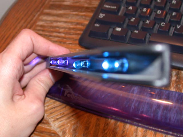
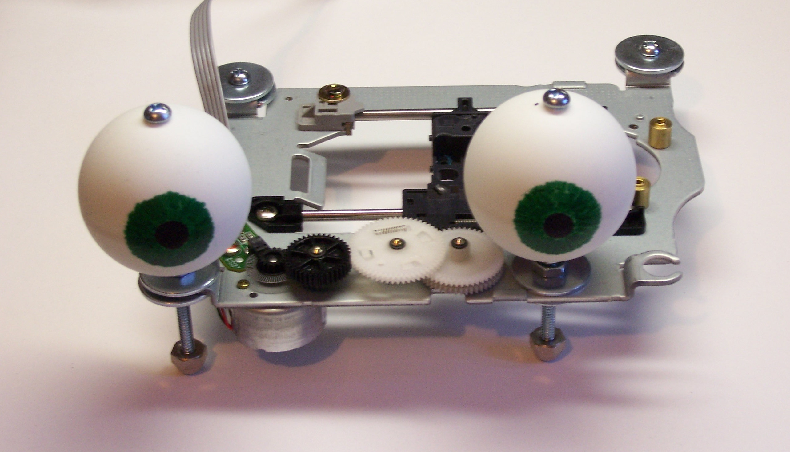
Back in mid-February, I wanted to demonstrate motor control with the LogoChip to class, but it’s hard to see what a motor is doing unless it’s geared down and attached to something. I decided to make googly eyes that could look around, and here’s how I went about it.

Motorized googly eyes

CD Read Sled

Although the motion of each individual eye is rotary (right to left; these can’t look up and down), to synchronize their actions, I needed linear motion.

Digression: Predator species have eyes on the front of their face, to triangulate the distance to their target. Prey have eyes on the sides of their heads, to keep the widest possible view of their surroundings and watch out for predators. Predators’ eyes generally move in synchronization. Of course, they may look slightly inward when watching a nearby object (binocular convergence; think of looking cross-eyed at your nose); but for a simple model like this, two eyes always looking in exactly the same direction is adequate.

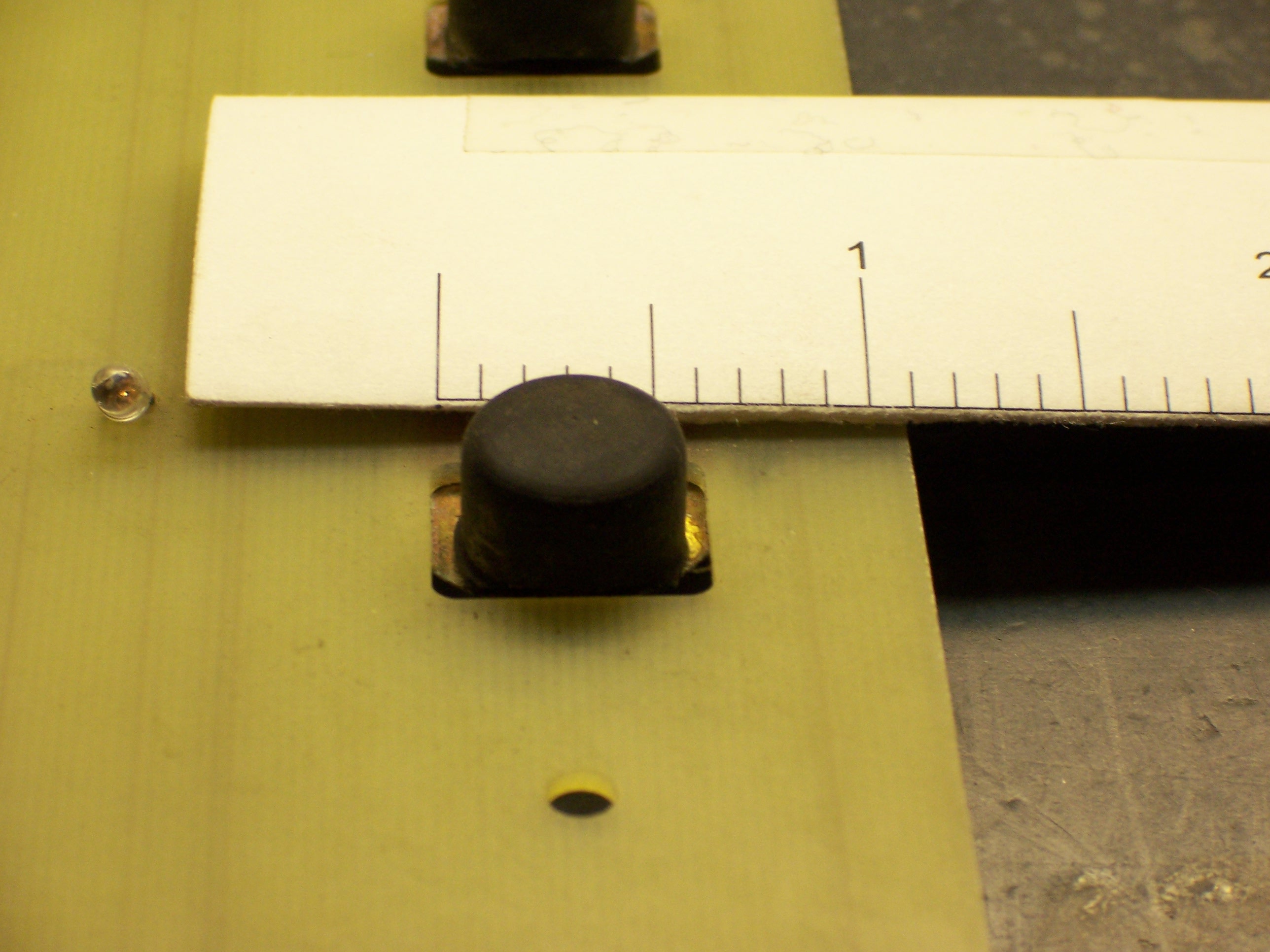
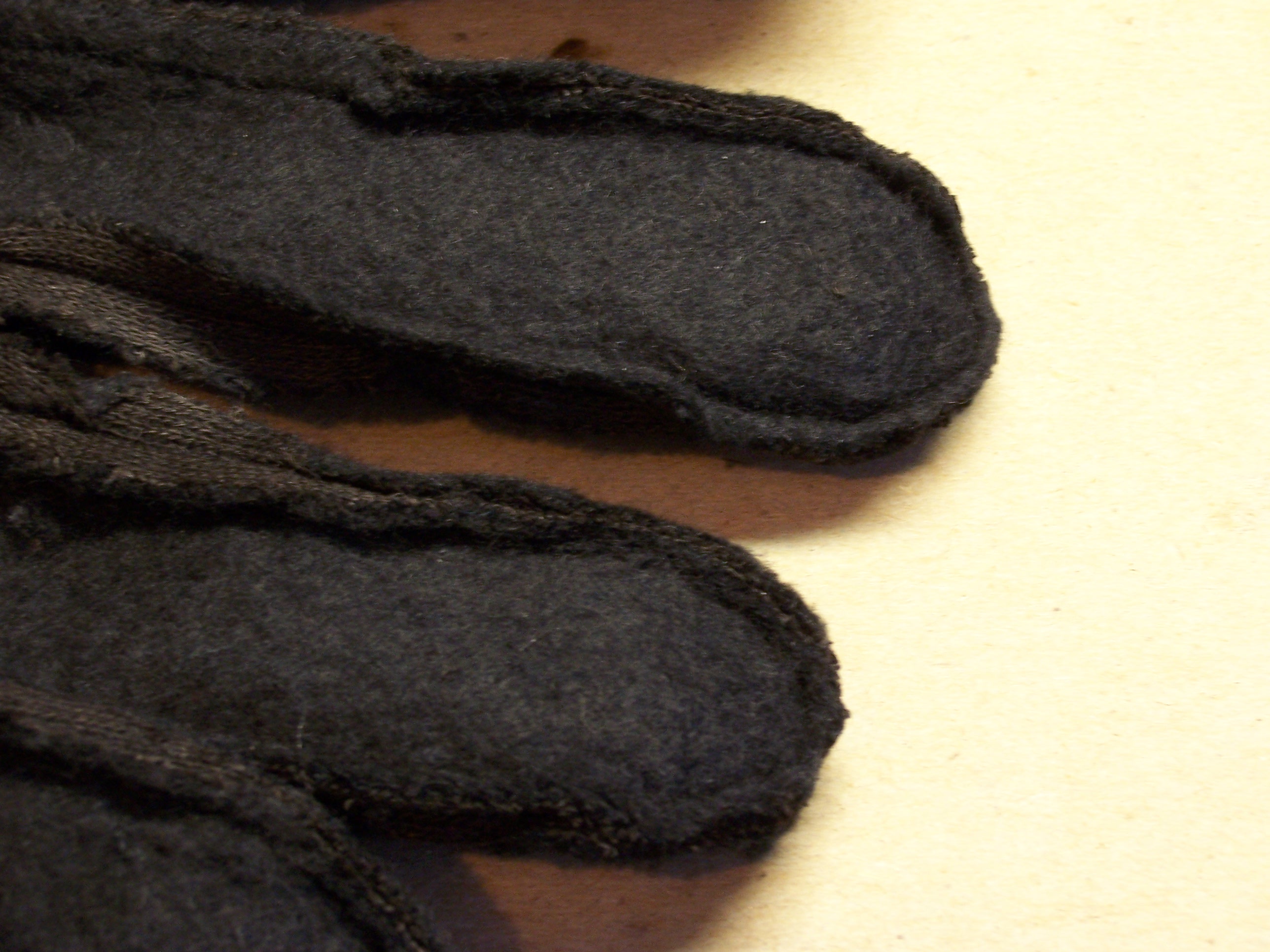
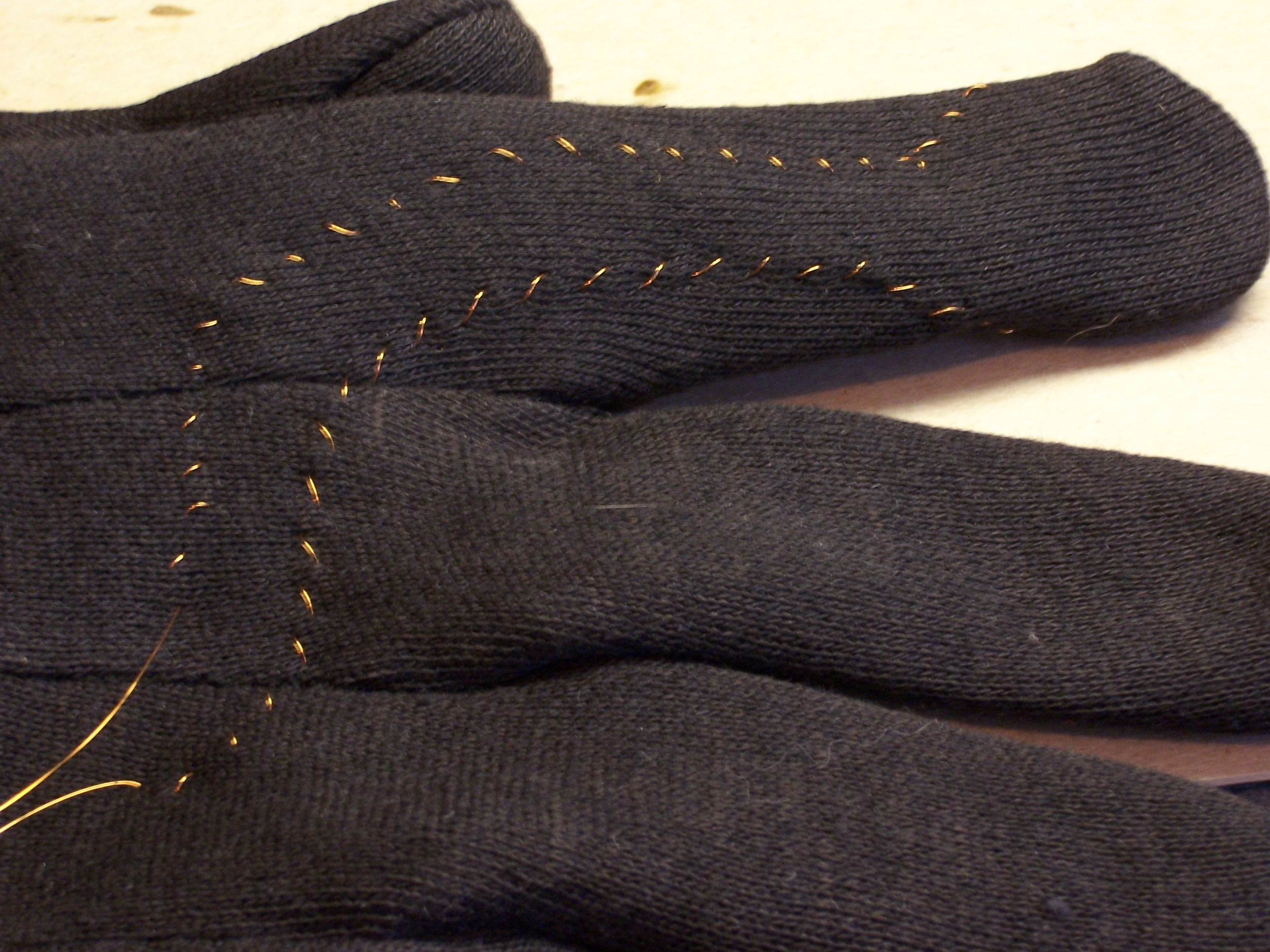
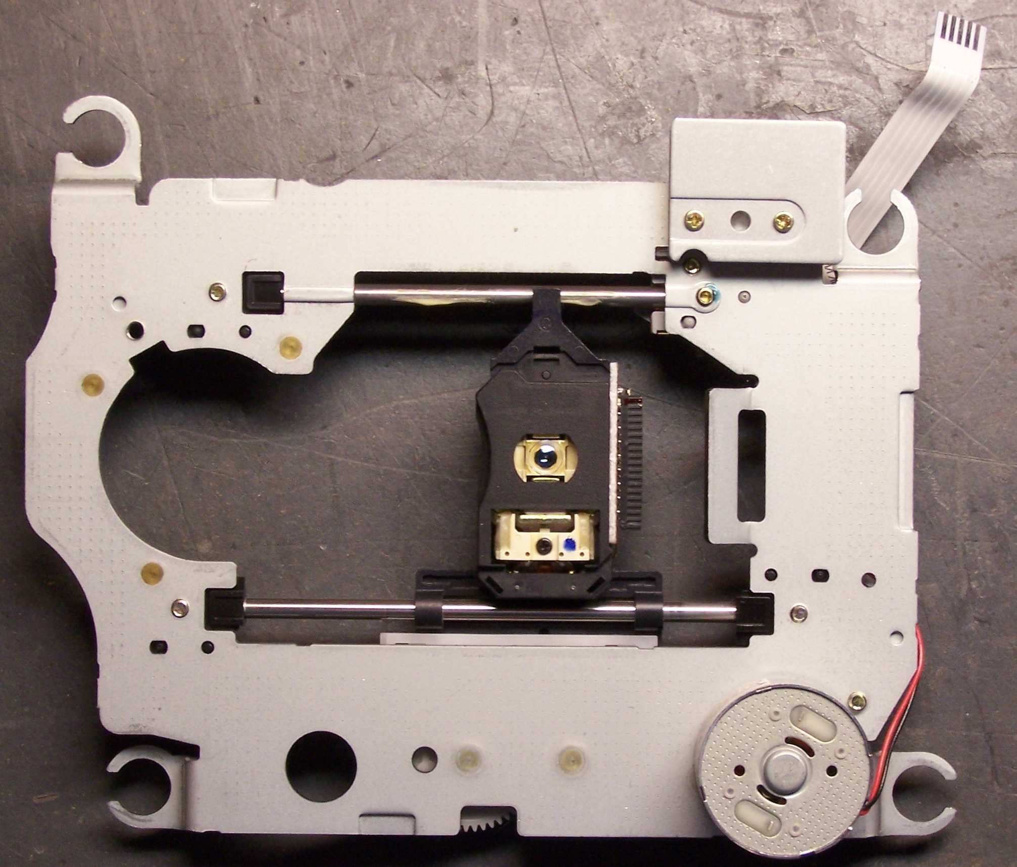
I figured my best shot was something from a dead CD-ROM drive, so I went down to examine my stash. What I call the read sled assemblies looked the most promising–they’re the ones that move the read head in and out along the radius of the disc to find the right position to play. The tray motors might also work, but the trays have a good 5″ range of motion. The ∼2″ range of the read sled seemed much more useful.

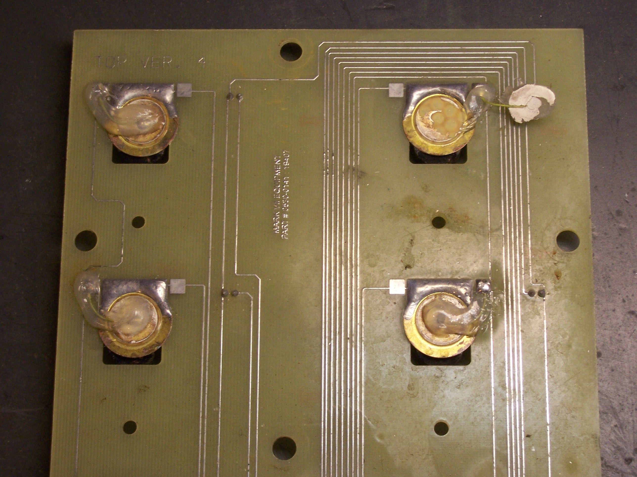
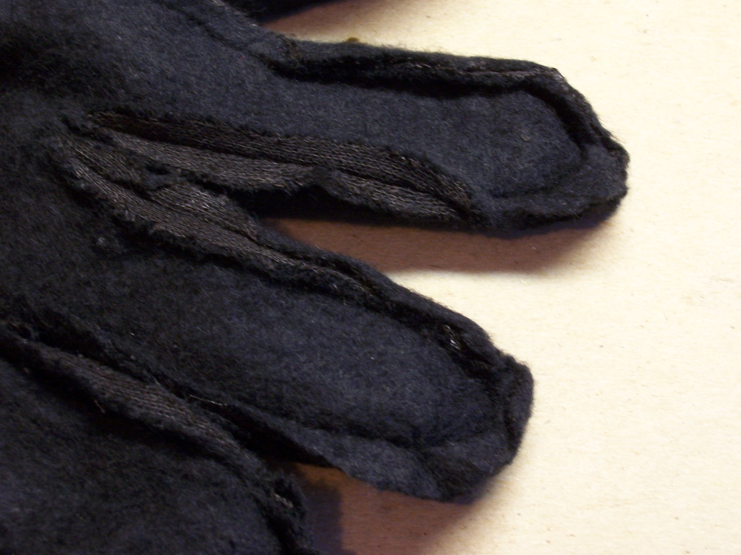
Several of the assemblies I examined used a stepper motor, but I wanted to demonstrate a simple DC motor, so I kept looking. Finally I came across this one, which had a DC motor (on the underside), a nice geartrain, and an optical encoder (the faint grey circle between the green PCB and the medium black gear) to determine the position of the sled.

CD-ROM drive read sled assembly

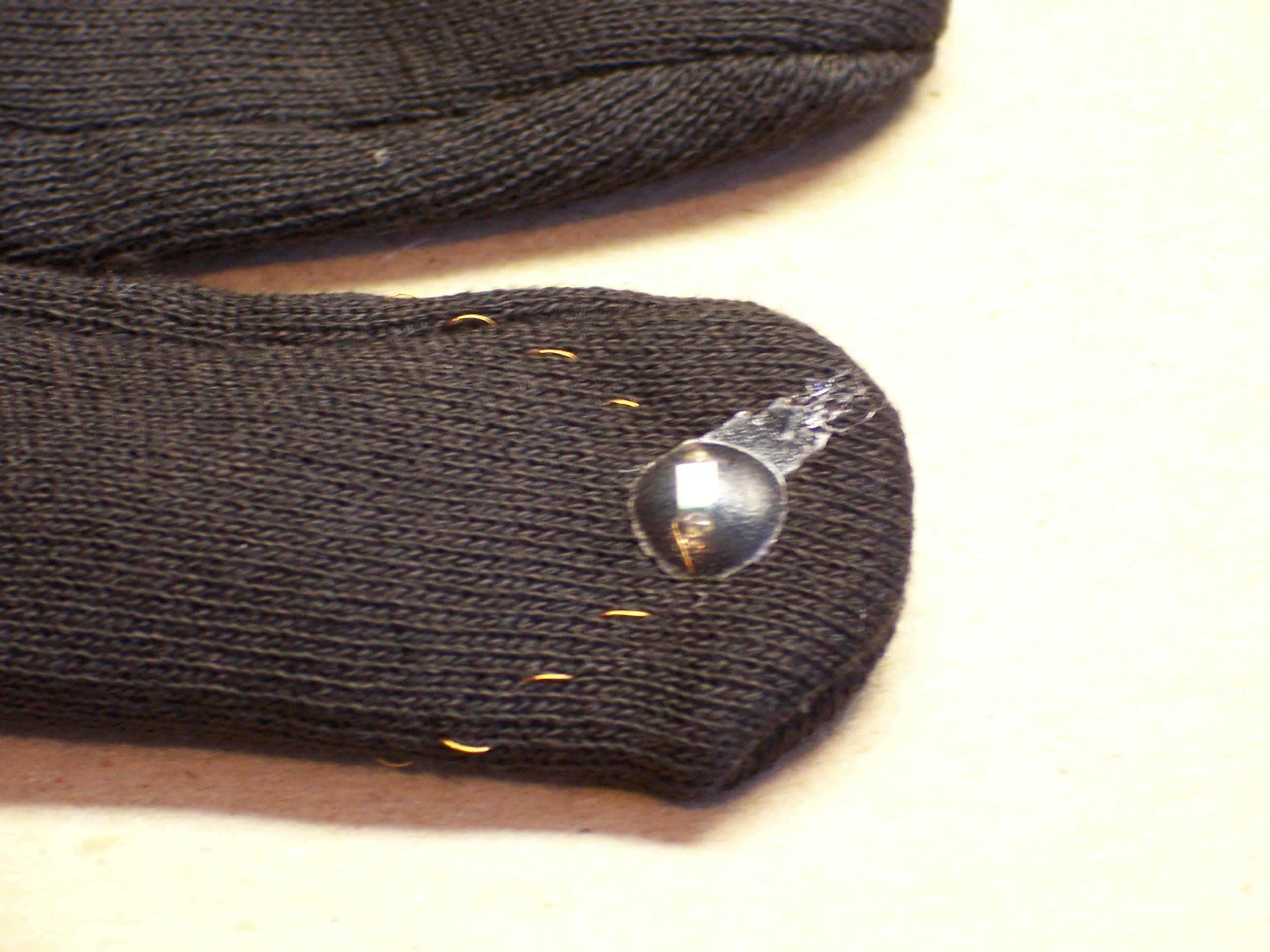
The motor was mounted from the back side, and the optical disk was press-fitted to its shaft.

CD-ROM drive read sled assembly, reverse

Reverse-Engineering the Optical Assembly

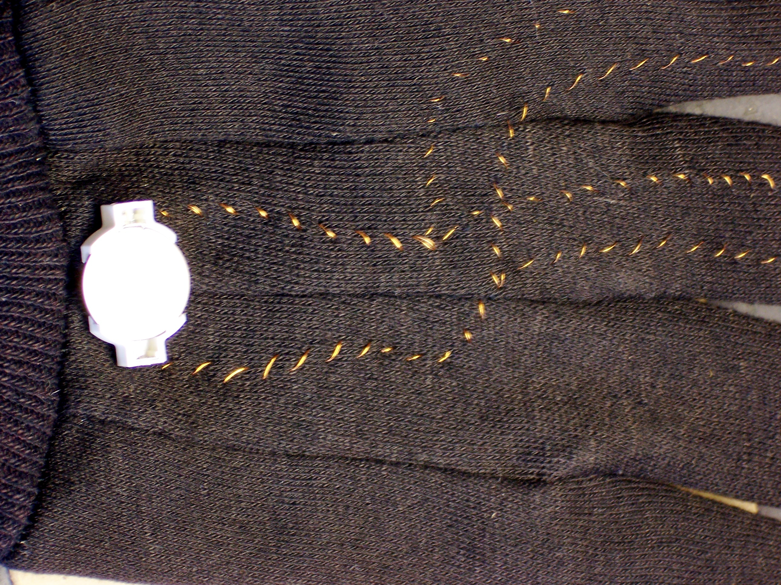
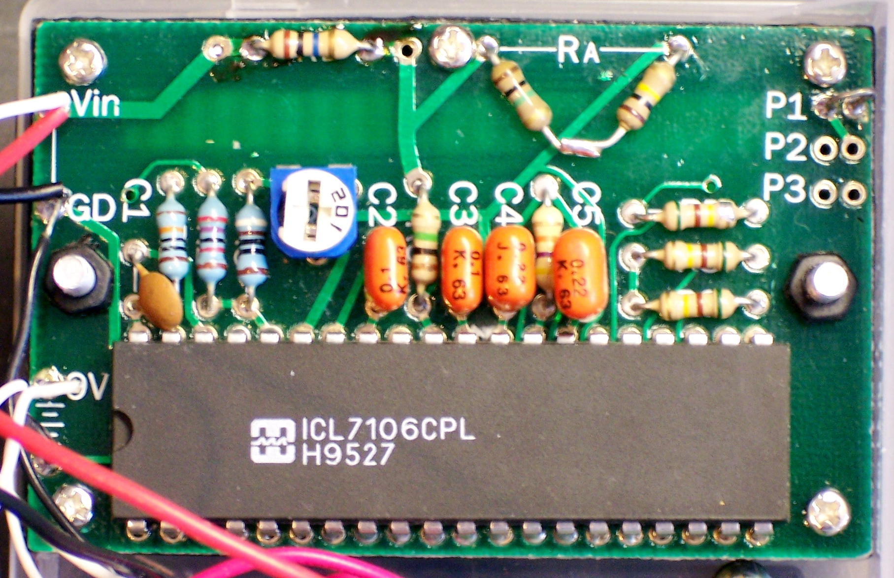
I was interested in trying to reuse the optical assembly so that I too (well, my program) would know where the sled was, so I desoldered the flex pcb ribbon cable and set about figuring out the connections on the PC board.

Optointerruptor and interface PCB

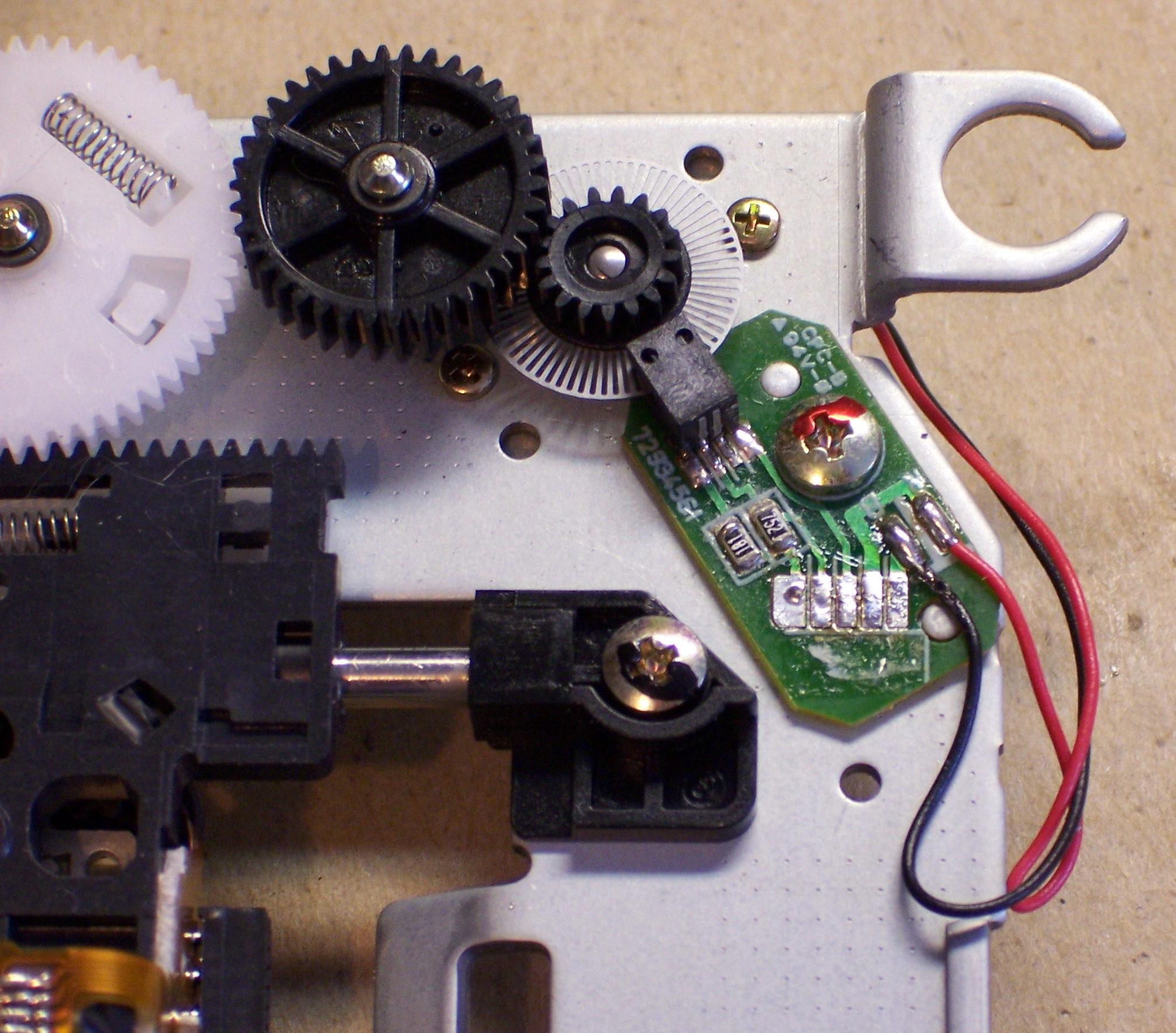
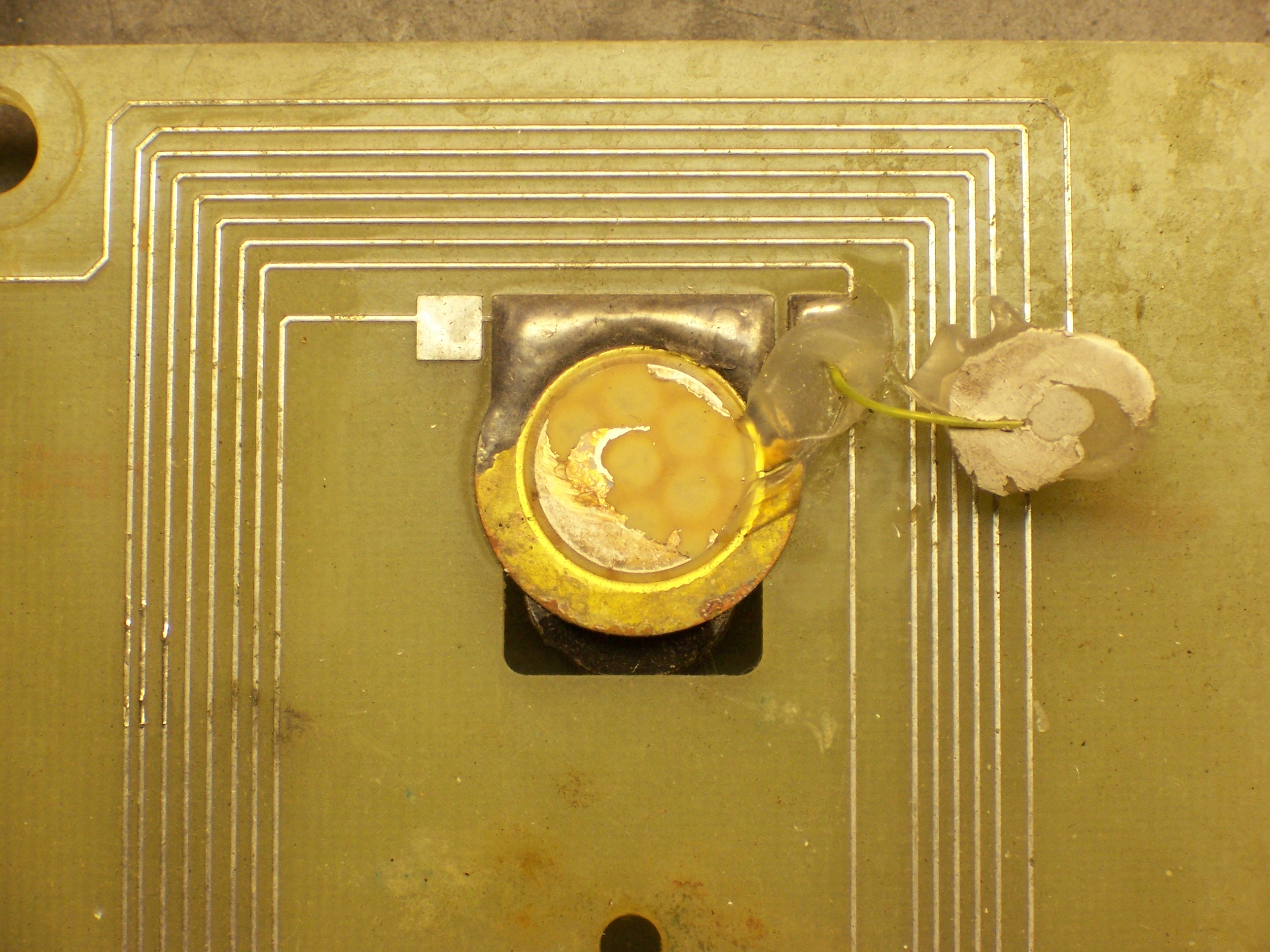
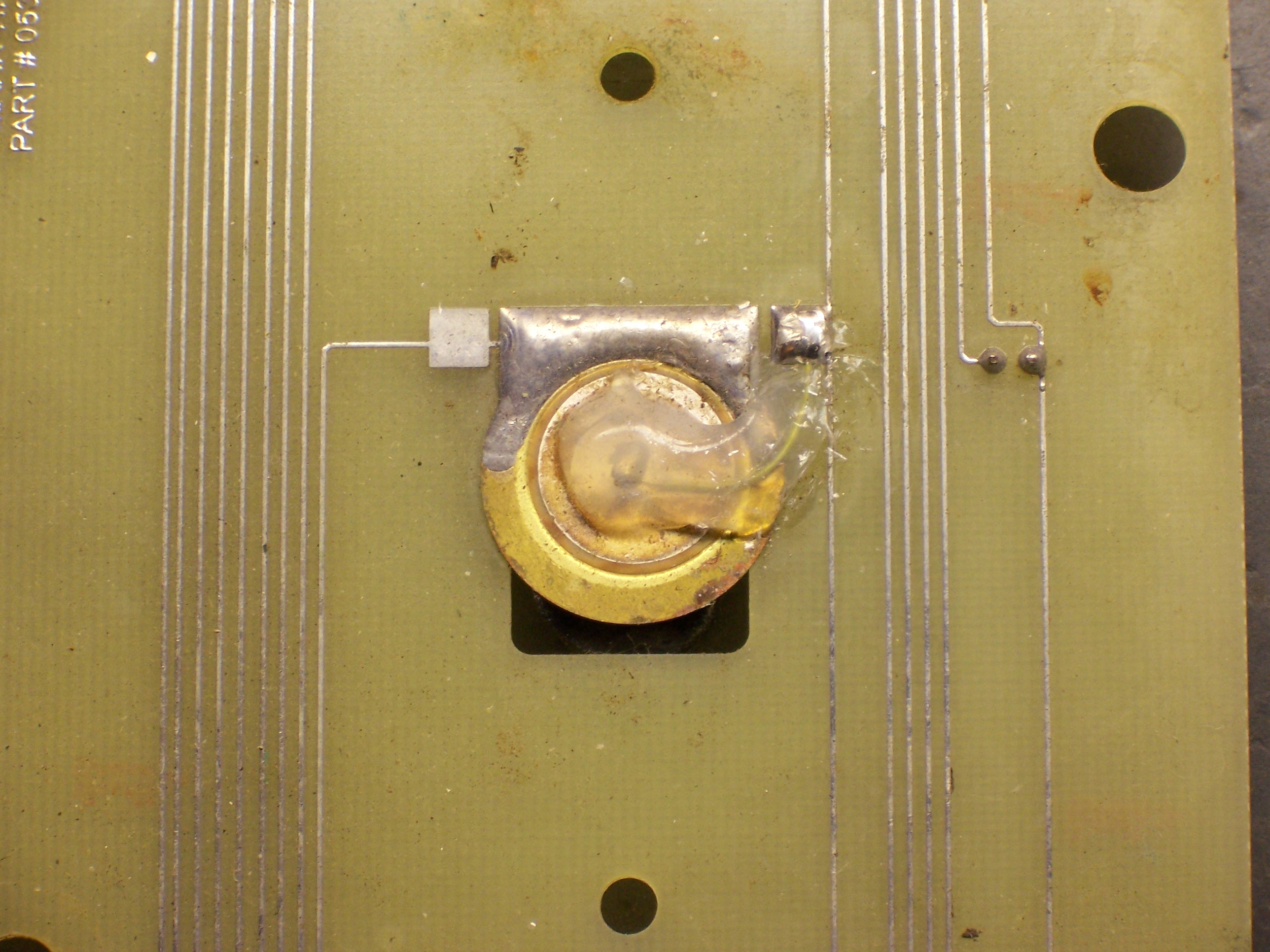
The larger black rectangle that overlaps the optical disk was obviously an optointerruptor–one side has an LED and the other side some kind of optical sensor. When a hole in the disk passes between them, light is transmitted; when a bar passes between, the light is interrupted, and the receiver can tell the difference.

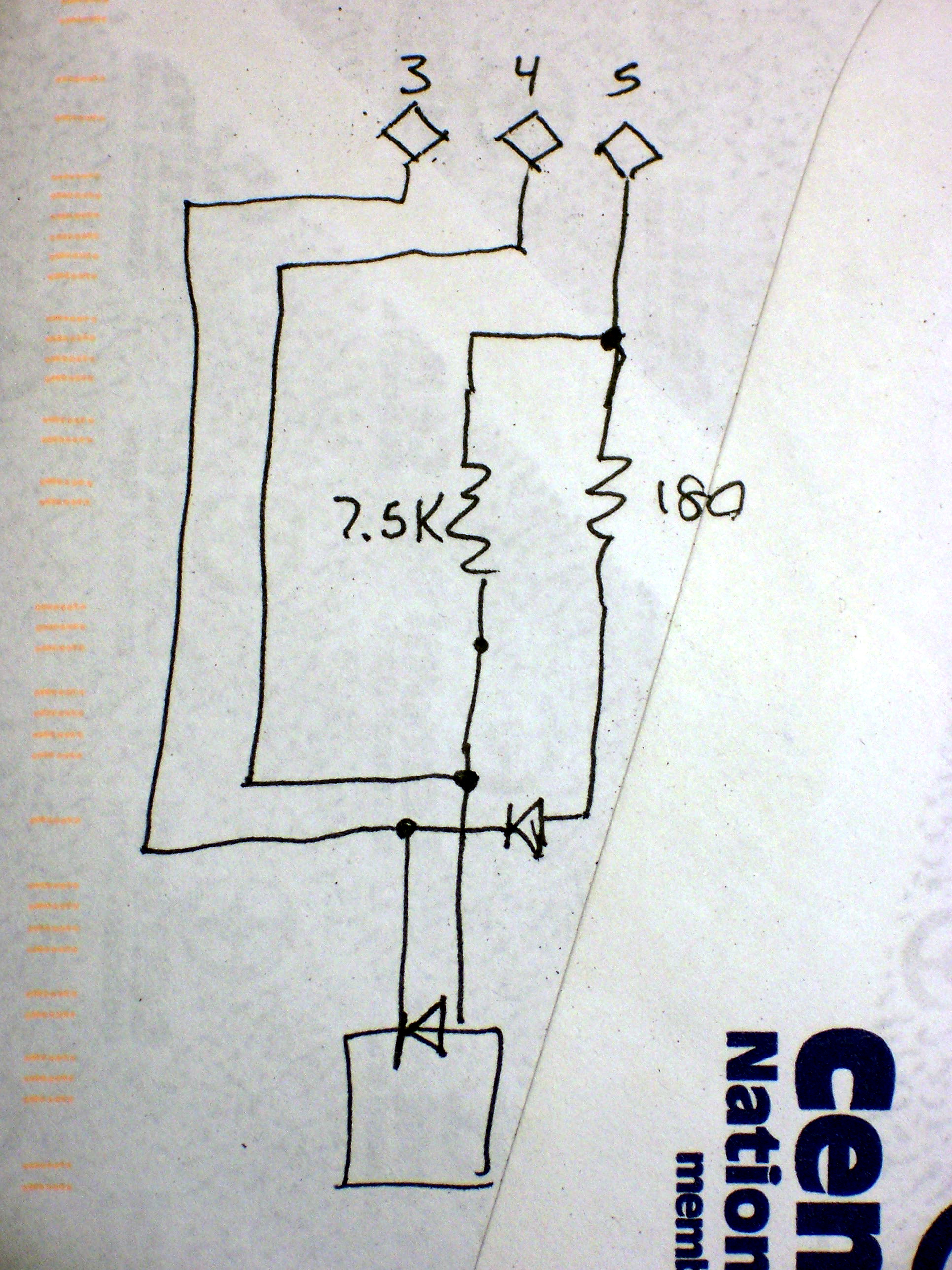
The two smaller black rectangles (southwest of the screw head) are surface-mount resistors, reading “181″ (180Ω) and “752″ (7.5KΩ). I could visually follow some of the traces (the light green lines) on the board, but I got lost with exactly what happens underneath the resistors.

I assigned numbers to the five solder pads from the cable, arbitrarily numbering from the outer edge of the board. (In retrospect, that was incorrect–the pad to the left in this photo is shaped differently than the others; that makes it pin number 1. Ah well.) Then I made this table (actually edited here on my blog–all the notes have been sitting around for six weeks, and it’s only the narrative that I’m adding later) describing where each pin went, to the best of my visual acuity.

Pin Connection
1 motor black wire
2 motor red wire
3 interruptor
4 interruptor end of 7.5KΩ resistor
5 both resistors

Pins 1 and 2 obviously run to the motor, and it was pretty clear that they didn’t have any connections to pins 3-5. So I used my ohmmeter to measure the resistance in each direction between each pair of pins out of 3-5. I got this:

4 → 3: 50KΩ
3 → 4: ∞
5 → 3: 40KΩ
3 → 5: ∞
5 → 4: 7.5KΩ
4 → 5: 7.5KΩ

It was obvious that pins 4 and 5 were connected directly via the 7.5KΩ resistor. It was also apparent that there were diodes from pin 4 to 3 and from pin 5 to 3. That gave rise to this diagram:

CD read sled connection diagram, reverse-engineered

Which made a lot more sense once I redrew it like this:

CD read sled connection diagram, redrawn

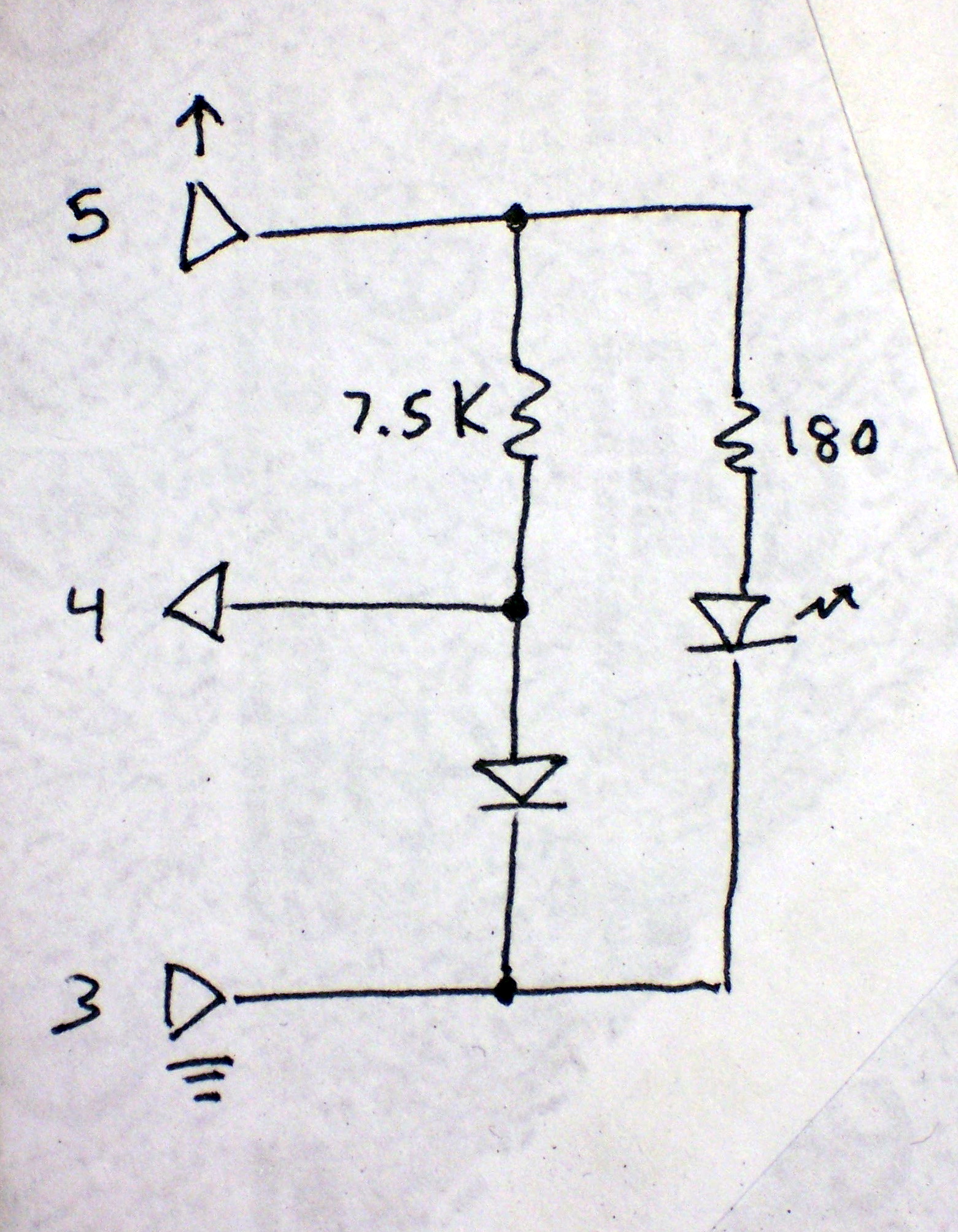
Pin 5 is the supply voltage, pin 3 the ground, and pin 4 the readout of the voltage divider between the 7.5KΩ resistor and the photosensitive diode. Voila!

Using the Optical Encoder

A 180Ω current-limiting resistor with a 5V supply would give ∼24mA of current through the LED, and that seemed a little high. I’m guessing that part of the circuit ran on 3.3V, making the LED current ∼14mA–a more reasonable value.

I wanted to shoot for 15mA, so 4.3V / 15mA ≅ 290Ω, of which 180Ω was already in the circuit, leaving 110Ω to add. I had a 120Ω resistor in my bin, so 4.3V / (180Ω + 120Ω) ≅ 14mA, which was close enough. I used the 120Ω resistor to wire pin 5 to the 5V supply, placing it in series with both diodes. (I figured its impact on the 7.5KΩ resistor and photodiode whould be negligible.)

Turning the encoder wheel very slowly and carefully and reading the voltage at pin 4 yielded a minimum voltage of .77V and a peak of 3.4V. (Alas, I don’t remember which was when the light was blocked and which when it was passed . . . probably the photodiode conducted and pulled it down to .77V when light was passing . . . but I don’t know that I really care.)

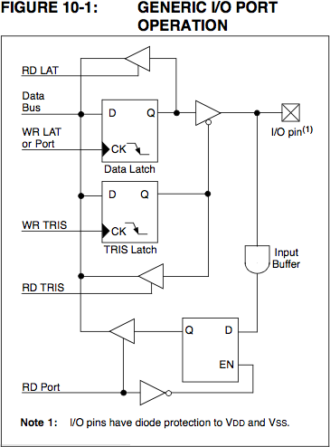
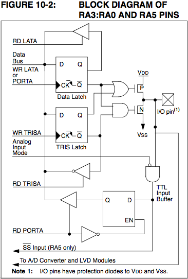
I didn’t really want to have to use an A/D converter input and deal with a 10-bit numeric value when all I needed to know was whether the light was blocked or passing. But I wasn’t wild about feeding a continuously varying analog voltage into a TTL input–it tends to make them overheat. Happily, the PIC datasheet (p. 102) revealed that pin A4 has a Schmitt trigger input, and my problem was solved.

A Schmitt trigger has hysteresis–the input signal has to rise above a certain point (the “high-water mark”) before it reads high, then fall below a lower point (the “low-water mark”) before it reads low. It’s intended for reading digital values from analog signals, it was exactly what I needed, and it worked exactly as desired. I fed the optointerruptor signal into A4 and got clean, predictable digital results.

Next Steps

That’s probably long enough for one post. Next: Building the eyeball assembly and programming the motor.

Piezo Elements for Percussive Input

April 1st, 2007 by Keith Neufeld

Harry Partch and Piezo Instruments

Lauren Hirsh, a WSU percussion student, WSU Internet radio goddess, and all-’round CRATEL regular, is involved in a performance of Harry Partch compositions this spring. Partch composed for new instruments he created, and the percussion department is attempting to build at least one or two of them for the concert. Lauren is taking on the task of building one, I believe the boo.

The boo is a marimba-like instrument made from tuned bamboo tubes arranged in six ranks. Rather than try to reproduce the tonal qualities of the original instrument through physical means, consideration is being given to building an input interface and using electronic reproduction of the boo sounds. In other words, Lauren wants to build a synthesizer keyboard shaped like a marimba. And several of us involved in CRATEL are intrigued by the challenge.

Tom McGuire has done all the work so far. He got a piezo element and hooked it up to the LogoChip. When you strike it, it generates a voltage; he’s working on capturing the voltage in a capacitor until the LogoChip can come along and poll it. The capacitor doesn’t have a drain resistor; he’ll turn the LogoChip port into an output at 0V after he’s read it, to drain it manually. In other words, he’s making a piezoacoustic version of the CCD camera. Brilliant!

Here’s a picture Tom sent of the element attached to a PVC faux bamboo tube:

Tom McGuire's piezo element interfacing

Sources

Tom has a few piezo elements, but maybe not enough for the whole instrument (even though Lauren only wants to construct a couple of ranks). But tonight, I mentioned the situation to my friend Joel, and he rooted around to bring out four boards with a dozen piezo elements each, which he’d be happy to donate as long as they don’t all get used up.

Piezo board, back

Each piezo has a rubber-covered button stuck onto the front–Joel thinks they may have come from an ATM or some other heavy-duty input system. It doesn’t feel like they can be removed easily, and I don’t know whether that will prevent them from being useful.

Piezo element, knob on front

Worse, they’re a bit corroded, and trying to remove the silicone that holds down the wire tends to rip the foil right off the back. I don’t know if there’s enough salvageable here or not, but I wanted to post the pictures to let Tom have a look.

Piezo element, back, torn

One I haven’t torn yet:

Piezo element, back

LED Gloves

April 1st, 2007 by Keith Neufeld

Background

Steve Wilson is a graduate student involved in WSU’s CRATEL (Center for Research in Art, Technology, Education, and Learning) program, and his video synthesizer was sponsored for further development in last year’s BETA (Bridging Entrepreneurship, Technology, and the Arts) competition.

One of Steve’s challenges for his video synth, and an interest in general, is creating expressive interfaces to electronic instruments. He describes it in a post to the Technology: Art and Sound by Design class mailing list. Basically, it comes down to the idea that acoustic instruments offer an immense amount of control over the sound that comes out through physical manipulation, and electronic instruments tend to offer much less control, and through mechanisms mainly like knobs and sliders.

While brainstorming with Steve about his synth, several of us came up with the idea of an interface like a plasma globe, which you control by moving your fingers over the surface. A cheap videocamera inside could watch what was happening and control the action.

Apparently a group of engineering students have been working on the globe subproject for six months without much progress to report. Although their difficulties seem to be mainly lack of organization and lack of time, others of us had talked about how clear an image might be obtainable on the camera with the globe lighted from the inside or outside.

Finally it occurred to me (while driving home from work) that gloves with LEDs on the fingertips would make lighted spots that should be very easy to see from the inside of the globe. Different colored LEDs on different fingers would allow the driver software to identify the different fingers; and pressing the LED against a translucent surface will produce a sharper point than holding it further away, so it might even be possible to determine approximately how near a fingertip is to the globe’s surface. And if made properly, the glove could be worn without impeding other use of the hand–just adding lights for the globe.

Time to prototype.

Gloves

I was hoping to find a cheap lycra glove to make something like the original Dataglove. (Yes, I have a Dataglove system. No, you can’t play with it.) What I found instead was certainly cheap, but knit cotton instead of lycra. Heck, for 96¢, it was good enough.

When I put the gloves on, I could feel that they’d been assembled somewhat sloppily. Inside-out, it was easy to see that there was a lot of extra fabric inside the fingers outside the stitching:

Fingers need to be trimmed

So I trimmed it a little closer and more evenly around the fingertips, for better fit and comfort.

Fingers trimmed

LEDs

I wanted to use surface-mount technology (SMT) LEDs, so they’d fit flat against the glove surface. The ones in my stockpile are out of broken digital office phones, used to light up beside the line appearance and feature buttons.

I wanted to be sure I knew the polarity before I started attaching things and soldering them together, so I tested first with my meter. The LEDs actually lit with the small amount of current it supplies, which was kind of cool. Curiously, the green LEDs have the anode on the end with the cut corner, and the red LEDs have the cathode on the end with the cut corner. On each LED that I identified, I marked the anode end with the color of the LED. (The ones on this sheet are tinted to indicate their color, but the ones I’d already removed weren’t.)

The phone flex-PCB has a 300Ω resistor in series with each LED, so I tried out a couple there on the strip. Nice and bright.

Testing an SMT LED

Soldering the LEDs

My plan was to solder wire the LEDs, then sew the wire through the glove to the back side, where I wanted to attach a battery holder. I got out some fine wire, scraped off the enamel insulation, wrapped it around the fly leads on the LED, and soldered it up.

Soldering the SMT LEDs

Sewing

After I had both wires soldered to the LED, I threaded one at a time through a needle, held the LED about where I thought I wanted it on the fingertip, and started sewing. The goal was to get the wire from the tip of the finger to the back of the hand without leaving any large loops that might snag on anything, and without reducing the stretchiness of the glove. The latter factor called for a zig-zag stitch, which with a single thread looks like a running pattern of slash marks.

LED on second finger

Once I got the wire stitched around to the back side, I followed along the back of the finger and then curved toward the center of the back of the hand.

Stitching from the back of the finger toward the battery

Glue for Protection

I needed something to protect the LEDs on the fingertips so they wouldn’t snag. When the wires were safely stitched around out of the way, I got out the hot glue gun, put on the glove, put a dot of molten glue over the LED, and pressed the glue into a perfectly-shaped dimple in a USB serial connecter that I lifted from the CRATEL lab. It soaked into the fabric a bit, adhered very well, and made a nice smooth bubble over the LED.

Glue bubble over LED

Well, mostly nice and smooth. Hot glue tends to stretch like pizza cheese, and I made a little boo-boo.

Battery Holder

For now, I settled on prototyping just two fingers, because I have only two colors of SMT LEDs, and because it seemed like enough for a proof of concept. I steered the appropriate wires onto the same paths and ran them up to where I wanted the battery holder.

Back-side stitching for two fingers

Then I clipped the wires short, scraped the ends, folded the glove over to get room to work, and wrapped the wires around the leads of a surface-mount coin-cell holder salvaged from a PC motherboard.

Soldering battery holder

I soldered them on, then folded the battery holder leads underneath so they wouldn’t poke through the glove and scratch up the hand. Laid back out, it looked like this.

Back of glove with battery holder attached

The Lights

I didn’t bother with a switch on the prototype–just pop in the coin cell and the LEDs come on. And because I’m using an old, small battery, I didn’t bother with current-limiting resistors–the internal resistance of the battery seems to be enough to limit the current to the LEDs.

Lighted fingers

Due to the idiosyncracies of my digital camera, the green LED on the index finger doesn’t look very green in this picture, but it really is. It’s a lot dimmer than the red LED, though; and I’m not sure why that is. Before going beyond a prototype, I’d want to pick current-limiting resistors to more closely calibrate the brightness of the different LEDs.

I don’t have a translucent globe to use, but I borrowed a hemispherical Tupperware bowl from my friend Lawrence’s daughters. (Don’t ask my why the girls have their own set of Tupperware–I really don’t know.) It works well enough to demonstrate the idea:

LED fingers through Tupperware

You can clearly see where the red LED is touching the bowl. Now all we need is a videocamera, some fancy software to track the lights, and an interface to a video synth. :-)

Seriously, all of those things are Steve’s domain. I just wanted to see whether I could throw together a working glove, and I think this’ll do.

Oh–and when you want to shut it off, you take out the battery and drop it into the thumb.

LogoChip Port A, setbit/clearbit, and analog inputs

February 16th, 2007 by Keith Neufeld

Twice before, I’ve run into problems with the lines on the LogoChip’s port A not working the way I expected–while programming an interface to the A6276 LED driver, and again when trying to interface to the DS1302 real-time clock. The second time I ran into it, I fixed the problem by changing port A out of analog input mode–but didn’t know why that made a difference. Last week, poring over the PIC18F2320 datasheet, I finally figured out what’s going on and why the analog input mode matters.

I was working on output routines for TASD’s Thing 3: Simple Outputs, and we’re using port A because it’s the most conveniently placed on the LogoBoard. Every time I’d do a setbit or clearbit command against a line on port A, all the other outputs would change to 0.

Tom McGuire had run into this problem recently, and worked around it by reading and writing the port A latch, LATA, instead of the port register itself. But that still didn’t explain why it was happening in the first place. So I sat down with the datasheet and looked at the port operation diagrams.

Generic I/O Port

PIC18F2320 datasheet, Figure 10-1

Here’s the diagram for a generic I/O port, from page 103 of the datasheet. Writing to the port or latch register (WR LAT or Port) puts data into the data latch, which is accessible by reading the latch (RD LAT) register. Additionally, when the data direction latch (TRIS latch) is in output mode, the data latch drives the I/O pin for output. Finally, the input buffer continually reads the I/O pin (even when outputting) and makes its current state accessible by reading the port register (RD Port).

So you can always write output data to the port or latch register; and when the port is in output mode, the last data written will be output to the pin. The last data written is always readable from the latch register; and when in output mode, the data is also readable from the port register.

Port A

Now look at port A, from page 103:

PIC18F2320 datasheet, Figure 10-2

The most visible difference is that the simple output buffer from the data latch to the I/O pin has been replaced by an arrangment of an OR gate, an AND gate, and N- and P-channel FETs. As far as I can tell, there’s no operational difference between the two–Figure 10-2 simply shows what’s happening in more detail.

More significant is the addition of the Analog Input Mode line controlling the input buffer–this is the crux of my problem. When port A pins are receiving analog input, it doesn’t make sense to feed that input into a TTL register–in fact, it could cause excessive power draw and overheating. So the input signal is gated by the analog input mode before feeding to the port A read line (RD PORTA).

setbit and clearbit

The reason this matters is that the LogoChip’s setbit and clearbit commands are read-modify-write operators–they read the value of their target, OR or AND that value with a constant, and write it back to the target. When that target is the port A latch register, all works as it should–the latch is read directly back out the RD LATA line.

When the target is the port A data register, however, the current value is read through the input buffer, which is gated by the analog input mode line. When the pin is set in analog input mode, even though the data direction is set to output, the port data cannot be read because the gate is off, and always returns a 0.

So when setbit <bit> porta attempts to change one bit, it tries to read PORTA and returns %00000000 rather than the value of the data latch. It then sets one bit and writes the new (mostly-cleared) byte back out to the port A data latch–clearing every other bit of port A in the process.

Workarounds and Solution

Two workarounds are obvious. Tom’s method was to manipulate the port A latch (LATA) instead of the port A data register (PORTA). The latch can always be read and written directly, so this works flawlessly. My only objection is that porta is already defined as a constant in LogoChip Logo. I’m not wild about having to teach students to define a new constant for lata and then use lata, portb, and portc.

The second workaround is also simple. When using the LogoChip setbit and clearbit commands, clear the analog input mode on any pin you want to use as an output. Because the order of analog input pins is predetermined (A0, A1, A2, A3, A5, . . .), this might mean rearranging the pinouts–you can no longer have A0 and A2 as analog inputs and A1 as an output, for example. But it’s a pretty easy method.

The true fix is equally simple. Where port A’s TTL input buffer is gated by (active-low) analog input mode, it should in fact by gated by (active-low) analog input mode OR (TRIS Latch is set for output). That is, any time the pin is NOT in analog input mode, OR the pin is set for output, pass the pin’s value to the port data read buffer. I don’t see any drawbacks to this solution, other than the cost of one additional OR gate.

Having taken the time to figure that out, I’m rather surprised that Microchip didn’t build the PIC that way.

LogoBoard

January 29th, 2007 by Keith Neufeld

Well, it’s time for another round of John Harrison’s Technology: Art and Sound by Design class–and oh by the way, this time I’m co-teaching. John’s doing the hard parts (course vision, blogs, wikis, etc.), and I’m doing the technology lessons for a while.

We’re calling them “Thing a Week,” sort of like another Thing a Week series you might have heard of, only different. On Monday and/or Wednesday, we introduce a technical topic, Friday we build it in the lab, and then next Monday we show it off.

So here’s the first one–me soldering up a LogoBoard, a carrier board for the LogoChip, designed by Tom McGuire.

Thing 1: LogoBoard Assembly (may move to here)

LogoBoard

Funny how a 15-minute soldering job turns into two and a half hours when you stop after every part to take pictures. :-)

Theremax, Part I: Circuit Board

January 22nd, 2007 by Keith Neufeld

A Theremin is an electronic instrument played by waving your hands in the air near a couple of antennae. It has matched pairs of high-frequency oscillators, and the change in capacitance due to the proximity of your hand changes the frequency one oscillator in the pair, causing “beats” (heterodyning) between the pair that form audible wavelengths. The Theremin was invented early in the 20th century by Leon Theremin, a Russian physicist. It’s the spooky sound you hear in the Beach Boy’s “Good Vibrations”–although that was actually recorded with an electro-theremin, a different instrument designed to mimic the Theremin’s sound.

I don’t know when I first became aware of Theremins, but I know I’ve wanted one at least since February of 1996, when Electronics Now published “Build this Theremin,” by John Simonton of PAiA Corporation. The full PCB layout and parts were published in the magazine, and PAiA has also sold their “Theremax” kit continuously since then.

And I finally ordered one.

Two, actually; my friend Cort wants one as well.

They arrived about a week later.

Board Assembly

Theremax kit parts

I bought the kit with the PCB and all components, and the separate partial case kit with the antennae and a nicely screened front panel. The full case kit was another $60, and I figured I could make a case that I’d be happy with for less than that. I think it says a lot about PAiA and their understanding of the hobbyist marketplace that they offer so many options, instead of forcing everyone into the same cookie cutter package.

The first thing I did was sort out all of the components. There are dozens of resistors and capacitors, a handful of transistors, four tunable inductors for the oscillators, pots and jacks for the panel (included in the parts kit, even if you don’t buy the panel), and miscellaneous bits like LEDs and ICs. They even threw in hookup wire to connect the PCB to the control panel, and a gator jumper for bypassing the volume control during one stage of hookup–literally every part you need to get up and going, except solder.

Theremax PC board, component side

Theremax PC board, solder side

Next, I took a look at the PCB. It’s a nicely-made single-sided board, with silk-screening on the top side for component identification only. I have only two small complaints:

  • The identifying marks for resistors and capacitors are under the component, so they’re no longer visible once the component is installed. I know there’s not a lot of extra room on the board for labels outside of the component footprint, but having to refer to a separate parts placement diagram really makes troubleshooting more difficult.
  • The resistors and capacitors are roughly numbered from upper left to lower right; but some of the numbers stray across the board, making it hard to locate the correct part. Maybe I’m too picky, but I really like an orderly numbering system during the assembly and troubleshooting stages.

Theremax PC board, resistors installed

The assembly instructions give a reasonable order for soldering in the components, which I mostly followed–jumper wires and resistors first,

Theremax PC board, diodes installed

then diodes. Note the blue diodes near the center of the board–germanium, with a lower voltage drop for increased sensitivity. I’ve read a nice description of how that aids the Theremin circuit, although I don’t recall it at the moment.

Theremax PC board, inductors and ICs installed

Here I deviated slightly from the instructions’ assembly order, and installed the ICs and inductors next. Because I don’t have a cool PCB holder, I solder with the board upside down on my workbench; and because of that, I prefer to install the shortest components first and work up to the tallest,

Theremax PC board, ceramic capacitors installed

which means doing the inductors before the ceramic capacitors,

Theremax PC board, electrolytic capacitors installed

and the electrolytic capacitors last.

Theremax PC board, transistors installed

The transistors are actually shorter than the electrolytics, but they cling to the board pretty well, thanks to the hole spacing being considerably wider than their lead spacing.

Control Panel

Theremax control panel

PAiA’s professionalism really shines here, and my photo doesn’t do it justice. This is a very nicely lettered control panel, as good as those on most of the equipment I own. I like the retro feel of the white paint on black brushed aluminum, rather than some glitzy decals on colored plastic that you might see these days.

Theremax control panel, back

I installed all of the potentiometers and jacks, twisting them as needed to try to get the hex nuts on the front to line up evenly. (I like to use the phrase detail-oriented.)

Theremax control panel, back with ground connections

The instructions say to run bare wire from pot to pot for the ground connection; but I’m not wild about bare wire (especially when it has to loop and could be snagged and pulled out to contact something else), so I put some clear heatshrink over it for sleeving. I also built up the LED assemblies–replacing the provided dark red LEDs with my own green LED for the power light, and a matching red LED for the gate trigger indicator.

Theremax PC board, fly wires installed

Then I soldered all the fly wires to the PCB. The assembly guide gave very specific lengths; but I think things must have shifted since that was first printed, because the wires had completely different amounts of slack once connected. I shortened some wires and should have lengthened others, and made notes about all the changes I made and further changes I should have made. Here are my notes about the colors I used and the lengths I’d recommend:

Board Panel Signal Length Modify Color
A R79-2 P trim 9 1/2 -1 blue
B R79-3 P trim + 9 1/2 -1 white
C R80-3 V trim + 5 +1 white
D R80-2 V trim 5 +1 green
E R81-3 timbre short sine 9 1/2 red
F R81-1 timbre short square 10 1/2 -1 blue
G lug GND 10 1/2 -2? green
H R82-3 pitch CV 12 1/2 blue
J R83-3 volume 9 1/2 red
K R84-3 velocity 9 1/2 +1 white
L J3-T velocity CV 11 -2 red
M J2-T gate 10 1/2 -1/2 red
N J2-R trigger 10 1/2 -1/2 green
R J1-T audio out 12 3/4 -2 1/4 blue
S J5-T volume CV 16 -6 blue
T J6-T mute 16 -5 white
+ S1-1 +12V 12 -1 red
SG J1-S SGND 5 +1 white
lug S1-3 GND 10 green

Theremax control panel, back with signal wires installed

The last thing I did in that batch of soldering was run signal wires within the back of the panel. The instructions gave this step at the same time as the ground wiring, but I wanted to wait until I had the fly wires chosen so I could maintain the same color wire everywhere a signal traveled.

Next Steps

By now, I’ve connected the fly wires to the control panel, built a case, and semi-mounted the kit in the case. I’ll post those pictures soon.

Battery Meter

January 7th, 2007 by Keith Neufeld

Battery Meter Prototype

Here’s a project that I’ve been kicking around for a long time (three years–I guess that’s not so long compared to some of my projects :-| ) and finally built–a battery meter. My friend/enabler Slim Cummings in Pittsburg gave me a couple of surplus 3-1/2 digit, .2V panel meters, and I thought they’d be perfect for testing the freshness of AA and AAA cells.

Meter

The meter was the inspiration for the project. It has a 3-1/2 digit (a 1 plus three 7-segment digits–1888) display, a configurable decimal point, and an Intersil ICL7106CPL LCD/LED Display, A/D converter chip. You give it 9V supply, a jumper for the decimal point, and a voltage input; and it samples the voltage and drives the LCD. It’s a very nice package that just begs to be used for something interesting.

Tester Case and Battery Holder

Parts to Build a Battery Meter

The physical aspects of the project actually took much longer than the electrical. First off, I wanted to find a case with the following characteristics:

  • The case would be held in portrait orientation.
  • The meter would fit across the width of the case, with the battery holder below it.
  • I could fit a 9V battery inside the case to power the meter.

I figured I’d find a plastic project case from Radio Shack with a 9V holder in one end and enough room for everything else to fit . . . no such luck. I figured I’d find something in my junk bin that I could reuse–I was coming close with some old and broken copper-to-fiber media adapters, but they weren’t quite right. Finally I stumbled across the idea of using the plastic case from a data backup tape, and I rummaged around until I found this KAO 8mm data cartridge case.

I’m not wild that it’s translucent–I don’t like seeing the guts of things when I’m using them–but it’s the perfect size. The meter exactly fits across the width, the 9V battery exactly fits in the thickness, and it’s in portrait format. Plus I guess it’s kind of cute opening the case like a cassette case to change the 9V battery.

Single AA Cell Holder

I picked up a single AA battery holder at Radio Shack a couple of weeks ago, and had to mod it a bit to fit it onto the case the way I wanted. The leads originally routed out holes in the ends of the holder, but I wanted them to go straight down through the case. Fortunately, there was already a hole underneath the terminal at each end (you can see the one at the right end of the above picture), and I was able to fish the wires through and tug them into position to make it work.

The holder also had tabs curving slightly around the front, to help hold the AA cell inside. Since I want to be able to insert and remove cells quickly, I removed the tabs by scoring the plastic flush with the rest of the front of the holder, then snapping them off. I also confirmed at this point that a AAA cell would make contact with both ends of the holder, even though it wouldn’t be held as securely. (AAA cells are shorter than AA cells, as well as thinner.)

Project/Tape Case with Mounting Holes

I drilled mounting holes in the case for the meter and battery holder, as well as holes for the wires to go through. The plastic was so soft, I didn’t even bother chucking the bits into my drill for most of the holes–I just turned the bits a few rounds with my fingers and I was through the case.

Stepped Drill Bit Set

I did get to use my stepped drill bit set to enlarge the meter’s mounting holes–the bezel’s posts have larger-diameter plastic shoulders at the base, my mini-drill doesn’t have bits that large, and the stepped drill bits do an excellent job of enlarging while remaining concentric with the pilot hole.

The last tricky bit of work with the drill was the big ugly hole in the center of the picture of the drilled case. I needed a power switch for the meter, but I was loath to have to have to slide a switch or press a button every time I wanted to use it–I wanted it to spring to life when a cell was inserted to test. Plus for reasons to be described a bit later, I planned for a pushbutton on the front already, and I didn’t want to have two.

The solution was simple enough–a pushbutton switch inside the battery holder, actuated by the insertion of the cell itself. I salvaged a tiny microswitch (“nanoswitch???”) from a dead CD-ROM drive (a limit switch from the optical sled), reamed much too large a hole in the case and battery holder, poked the switch in from underneath, and hot-glued it in place.

Meter Wiring

Digital Panel Meter, Component Side

The meter board is built for a range of 0 – .1999 (.2) V, but has pads to set the placement of the decimal point and to provide your own voltage divider to adapt for other ranges. The documentation gave the resistor values to adapt for 20V and 200V, from which it was easy enough extrapolate the nominal values for 2V operation: 9MΩ and 1MΩ. Well, I have 1MΩ resistors on hand, but not 9MΩ, and certainly not precision.

Fortunately, 9:1 ≅ 10:1.1, so I put a 10MΩ resistor into the pads for RB (upper left) and chained a 1MΩ and a 100kΩ in series between the pads for RA. (Those lap-soldering skills from a summer of module assembly at IFR Systems do come in handy.) Also fortunately, the calibration potentiometer had a generous range, so I was able to work around the 1% difference from the nominal ratio.

I also guessed (correctly) that the proper position for the decimal-select jumper was P1, which was missing from the voltage range chart.

Assembly

I had one more set of components to add, but I couldn’t resist wiring it up to see how it worked so far.

Battery Meter, Component Side

I soldered the 9V battery clip’s ground lead to the ground connection at the lower left of the meter board, the positive lead to the microswitch glued into the AA holder, and the normally open (NO) lead from the microswitch to the supply connection on the meter. I also soldered the AA battery holder’s leads to the Vin connections at the upper left. If you look closely enough, you may see that I just tack-soldered them in place with a lot of exposed wire a the end; I plan to come back and organize the wiring more carefully, and didn’t take a lot of extra effort at this point.

Meter in Action

Battery Meter in Action

And it works as planned! Not that there was much surprise, but it’s still nice when a project comes together. I was also pleased that the (undocumented) position of the decimal point was correct. Further, I was hoping to avoid cutting a large hole in the box for the panel meter; and I find it adequately legible reading through the nearly transparent case, without a hole.

I put a AA cell into the holder, the switch activated beautifully, the meter sprang to life, and I had a reading of the AA cell’s voltage. I measured the cell’s voltage in situ with my best voltmeter, calibrated the panel meter’s reading via the potentiometer on the back, and measured with my good meter once more to make sure the voltage hadn’t drifted while I was adjusting. Good enough!

Load Testing

Finally, I drilled two more small holes in the case, poked a pushbutton switch through (in the lower left of the above photograph), and wired a 10Ω resistor in series with the switch, and the switched resistor in parallel with the AA holder. From my first inspiration for this project, I’ve wanted to be able to test cells under load as well as unloaded. I find that some cells I’ve owned–particularly, I believe, when they’ve lost capacity due to age rather than use–will show a relatively high unloaded voltage even though they have very few mAh left. I very specifically wanted to be able to test under load to identify this condition.

And it’s proved itself already. The cell shown under test reads 1.163V, which is by no means new, but might still appear to be usable in some types of devices. But when tested with a load, it drops immediately to ∼.8V and continues to fall toward .7V–not nearly as promising. In contrast, another cell I’ve tested measured ∼1.2V unloaded, but still ∼1.1V under load–very likely quite usable yet.

Sorting Batteries

I’ve already switched to using NiMH cells for all my projects and consumer hardware, but I have a number of alkaline AA and AAA cells around the house from the old digital camera and the Visor PDA, with no good idea which are fresh and which need to be discarded. (Y’know, it’s such a pain to test cells with a voltmeter and only two hands.) I can finally conveniently test and sort them into four categories:

  • Unused: Save for when I don’t have any rechargeables ready, or give with battery-powered gifts to nieces and nephews who don’t do the whole “rechargeable thing.”
  • Still strong: Save for my LED flashlight, which seems to get quite a bit more life out of used cells than do incandescent lights.
  • Weak: An interesting problem. They still have some energy stored, but not enough to use in traditional portable devices.

    I’m planning to build a “Joule thief,” a clever and tiny transformer feedback single transistor inverter that claims to be able to “provide a week of continuous low level light from a battery that would normally be considered dead.” Maybe I’ll end up with a bunch of “electronic candles” sitting around for the next ice storm; who knows.

    Update: Here’s another Joule thief project.

  • Dead: Take to work and toss into the battery recycling bin. (And scrounge “weak” cells out of the bin to take home and make more “candles,” har har! Just don’t tell my wife that I’m stealing other people’s dead batteries now . . .)

Credit

A huge thank-you to my friend Slim, who gave me the panel meters that started this all; and who’s always generous with his vast experience and equally vast stores of electronics surplus.

LED Wrist Rest

January 3rd, 2007 by Keith Neufeld

Last fall, my friend Jeremy and I were killing time at Best Buy when we ran across this blue gel keyboard wrist rest. He was looking for a wrist rest anyway; and since we’re obsessed with blue LEDs, I offered that I could rig it up to glow. He loved the idea, and his wrist rest has been sitting at my house begging for attention ever since.

I’ve been tinkering around with ideas for a month or two, but finally yesterday I cleared some space on my workbench and got at it. There were four main components to the project:

  • The translucent blue wrist rest, which I hoped would have enough internal reflection to glow nicely
  • Blue LEDs, which I harvested from a string of Phillips Christmas lights
  • A USB cable, to supply power to the LEDs (Jeremy preferred USB so the lights would power on and off with the computer)
  • Some means of holding the LEDs in place

Glow Test

I’d been thinking I’d drill some holes into the wrist rest to embed the LEDs, but I wasn’t sure quite what the effect would be. I started testing by putting a couple of LEDs in my LED tester and shining them into the gel pad from different locations and angles, with disappointing results–they didn’t make any part of the pad glow like the edges of plexiglas (high internal reflections from the parallel surfaces) or milky plastic (high diffusion of the light beam).

So they kinda shine through instead of making the whole thing glow, and I just have to deal with that. On the other hand, that meant I didn’t need to bother drilling holes into the gel–I could butt the LEDs up against it and they’d work just as well. So I started thinking about etching a long, skinny circuit board to go across the back . . .

USB Cable

And meanwhile, tried to figure out where to get a USB cable to sacrifice. USB cables cost more than it seems like they ought to, so I was asking around for a dead USB mouse that I could salvage. I really wanted a black cable, to disappear on a dark desktop; and I really wanted a skinny and supple cable, to route well.

Then a couple of guys at work gave me a USB hot plate, I kid you not. It was from a trade show and was supposed to keep a coffee mug warm–which, no surprise, didn’t work out so well, given the limited current USB can supply. It had a skinny cable with silver foil inside–not black, but it still sorta fit with the theme. Perfect. Well, good enough.

Light Bar

Since it would have taken me a while to rig up a PC board for the LEDs, I was thinking about other ways to hold them in place and wire them together. I have some black plastic U-channel pieces about a foot long, which were supposed to be magazine or books supports for some wire cube shelves I bought, but which I’ve never used. Yesterday I cut the brackets off one, drilled holes in the back to poke leads through, and stuck four LEDs into it.

Several of the LEDs in the Christmas tree lights had 250Ω resistors already soldered to one leg, and that turned out to be a nice current-limiting value for a 5V supply, so I just left them in place. I daisy-chain soldered wires to the leads, connecting the LED/resistor assemblies in parallel, and attached the USB cable to one end. [Side note: In the USB cable, the black wire was positive and the white wire was ground. Good thing I checked first.]

Yup, I was soldering wires onto leads that were poking through (and touching) plastic. Surprisingly, I didn’t have much trouble with it–the wires were pretty clean, so they all soldered quickly, and apparently didn’t heat up much. I didn’t notice any melting plastic at all.

I used some big heatshrink to anchor the end of the USB cable in place and provide some strain relief (lower right end of the above pic), and the light bar was ready to go.

The LEDs are on the inside of the bar pointing out. That does a reasonable job of shielding the (annoyingly bright) light sources from direct line of sight, and plenty of light still makes it into the gel pad when the light bar is placed up against it.

This isn’t just a trick of the camera–it really does look like four beams of light aimed through the wrist rest. It’s not quite what I was aiming for, but isn’t a bad effect in itself.

The digital pic exaggerates the effect, but the four LEDs really are two different colors–two slightly more aqua, two slightly more violet. They’re all from the same string of LEDs, and I’d never noticed the effect before–I assume they’re from different manufacturing batches, with not particularly high quality control.

Credits

It wasn’t much of a project, but (1) it provided motivation to get some things cleaned off of my workbench; (2) it was itself part of the clutter on my workbench; and (3) it helped build momentum to get me back into tinkering. I’ve already started on my next project, which should appear here in a few more days.

Thanks to Jeremy Burkey for the photos. I forgot to take pics as I was working on it; and his camera did a much better job with the dark shot than mine would have anyway.

Arduino Circuits and Tutorial

October 15th, 2006 by Keith Neufeld

Tod Kurt is posting lecture notes from an Arduino class on his blog. It’s Halloween themed, and the two sets of notes posted so far look like a really nice introduction to electronics and the Arduino. Go, Tod!

EAGLE to PADS (FreePCB) Netlist Converter

September 16th, 2006 by Keith Neufeld

Based on a reader request, I’ve posted my EAGLE to PADS netlist conversion script, for drawing circuits in EAGLE and exporting them to produce in FreePCB (if the board is too big to draw in free EAGLE).

If you have questions, suggestions, or package translation contributions, please submit them as a comment attached to this post. If you’re viewing this post alone on a page, the comment box should be visible immediately below. If you’re viewing this inline in my blog, you should be able to click the “Comments” or “No Comments” link below to get to the comment box.