Archive for the ‘TechArt’ Category

Debugging a LogoBoard

Wednesday, April 18th, 2007

After the 2006 Technology: Art and Sound by Design final exhibit, Steve Atwood worked on building his own LogoBoard to use in his sculpture. He found that his board wasn’t working and was overheating, and asked for my help troubleshooting it. To my recurring shame, I’ve had his board ever since with very little progress to show for it. Time to rectify that.

The Board, the Symptoms, and Initial Efforts

Steve Atwood's LogoChip prototyping board

Steve built his circuit on a prototyping board with a .1″ perforated .1″ grid and connecting traces on the back, much like a solderless breadboard. The PIC microcontroller is in the center, with various components, connections, and wires surrounding it.

The main thing I knew when Steve gave me the board was that the LogoChip was overheating. I measured the resistance from the LogoChip’s power pin to ground pin and got some very low value like 4Ω, so I knew something was broken, but not dead shorted. I replaced his chip with one of my own and tested again; mine overheated and had the same resistance as well, so his problem wasn’t just that his chip had burned out.

And there it sat for a year.

Drawing the Schematic

In order to do any further debugging, I needed to determine and draw out exactly what was connected where, so I could examine the schematic and find what looked amiss. And the easiest way I’ve found to make a schematic from a PC board is to recreate the circuit in design software, building out the schematic and a reproduction drawing of the physical PC board at the same time. When the traces on the board drawing match the traces on the board, the schematic is correct and complete.

Working with two windows in EAGLE, I created a new project and added all of the components from Steve’s board. I had to fudge on the screw terminals and the crystal oscillator because I didn’t have library parts for them; but for a quick job like this I feel okay substituting a .1″ header and simply remembering what’s really going on. I carefully placed each component on the PCB diagram at the exact space corresponding to its placement on the real board.

LogoChip prototyping board, back side

Once I had the parts placed, I turned to the back side of Steve’s board and began tracing connections. I added a connection on the schematic for each connection on Steve’s board, switching frequently to the PCB editor to draw out the physical path of the traces whose connections had been entered so far. I drew it as a double-sided PCB; where Steve had jumper wires on the top, I made a via and drew a top-side trace.

PCB layout of Steve Atwood's LogoBoard

When I was finished, I had a fair facsimile of Steve’s board. Oh, there were some messy bits where jumpers overlapped and fly wires left the board, but it wasn’t too bad.

Schematic of Steve Atwood's LogoBoard

And more to the point, the schematic made it fairly easy to identify the problem. There are blocks of the circuit whose functionality isn’t identified (although it’s fairly easy to determine). But they’re not where the problem lies.

If you look closely at the power wiring to the PIC chip, you can see that it calls to have ground wired to pins 8 and 19 and V+ only to pin 20; but instead, ground is wired only to pin 19 and V+ is mistakenly wired to pin 8 in addition to pin 20.

Voila! Problem solved. Well, identified, anyway. I’ll leave it to Steve to rewire that.

Solder Splash

One more thing. When I was tracing the connections on LED2, the “run” light, I noticed solder splash between its upper pin and the ground bus. It’s at the right edge of the highlighted area, trying to hide underneath the blue jumper.

Solder splash on prototyping board

I haven’t checked it with a continuity meter, but it should be cleaned up to be safe. If I’m correct that it’s shorting the two wires, then the bicolor LED would still light one color (green or red) when port C3 (pin 14) is raised; but would remain dark when port C0 (pin 11) attemped to raise but was shorted to ground.

And with that, the board’s ready to go back to Steve.

CdS Photocell

Tuesday, April 17th, 2007

A cadmium sulfide (CdS) photocell is a passive component whose resistance decreases when light shines on it. CdS photocells can be used to detect when lights turn on, to orient things toward a light source (electronic sunflower), and to detect shadows passing across them.

CdS photocell

To use a CdS photocell, you put it in series with a resistor and put a voltage across them. This forms a voltage divider: the voltage at their junction is determined by the proportion of the two resistances. If you want brightness to increase the measured voltage, put the photocell on top; if you want darkness to increase the measured voltage, put the photocell on the bottom.

Circuit diagram showing two ways to connect a photocell

All that remains is to determine an appropriate value for the complementary resistor. Assuming you want output voltage to increase when brightness increases, the goal would be to make the output read as close to 0V as possible when it’s as dark as you expect it to be, and as close to your maximum voltage as possible when it’s as bright as you expect it to be.

To begin this calculation, I measured the resistance of the photocell (out of circuit) in light and dark conditions. With the photocell shown above, I found the following values:

450KΩ in the dark (my finger pressed over it)
36KΩ in average light
7.6KΩ in bright light (under my fluorescent desk lamp)

I discovered later that the photocell’s carrier PCB isn’t entirely opaque and a noticeable amount of light does leak in around the edges even when the face is covered. The resistance in true darkness would probably be even higher.

I decided to scale the photocell’s circuit to the range from darkness to normal room lighting, so calculating for a resistance range of 450KΩ to 36KΩ. Because this is only a single order of magnitude variation of resistance, I could already tell the voltage swing of the output wasn’t going to be as large as I’d like. I picked a 100KΩ resistor and estimated the voltage range:

5V * (100KΩ / (100KΩ + 450KΩ)) ≅ .91V
5V * (100KΩ / (100KΩ + 36KΩ)) ≅ 3.7V

So it has a swing of about 3V out of a 5V range. Not ideal, but it still provides a fair amount of resolution.

Finally, I connected the photocell to my LogoChip’s A0 input and confirmed its behavior by running print read-ad 0. I got a wide range of values out of the A/D converter, making this circuit quite usable for microcontroller interfacing.

I also posted a cookbook version of using the photocell on the TASD class wiki.

Making Googly Eyes, Part 2: Construction

Monday, April 16th, 2007

As noted in Googly Eyes Part 1, I built a demo back in February out of a CD-ROM drive optical sled assembly and a couple of ping-pong balls. In the earlier installment, I discussed reverse-engineering the sled’s electrical connections; now here’s how I rebuilt it to operate eyeballs.

I had thought I might find some googly eyeballs in the Wal-Mart craft department, for making big puppets or something. But all their googly eyes were the flat, button-like kind that just stick onto a surface, so I went with my fallback plan of ping-pong balls.

Drawing an eye on a ping-pong ball

I drew an eye onto two of them, with a black pupil and green iris. I didn’t mean to get the iris quite so dark, but at least I made it with radial lines.

Googly eye with bolt for axle

I located and marked the north and south poles of the ping-pong ball as carefully as I could, then drilled through with PCB drill bits. After stepping through several increasing sizes, I was able to use my stepped drill bits to make nice, round, even holes for the axle. I stuck a bolt through and threaded a nut up fairly close to the ball, so it could swivel but not move up and down much.

Googly eyes mounted to frame, front view

The sled assembly didn’t have the right sized holes in the right places, so I used big fender washers to make things fit. The eyeball-mounting nut is tightened against the fender washer, with another washer and nut on the bottom side. The bolts continue through the frame and act as legs to raise the underside of the carriage off the surface it’s sitting on, with cap nuts (acorn nuts) for feet to keep the end of the bolt from scratching.

This was actually a bit less than ideal, because the mounting hole for the right eyeball (left edge of the picture) is in a section that’s bent up and raised above the plane of the other holes. I tried compensating for the height difference with an extra nut under the left eyeball, but it’s still not quite right. Probably a washer in between the two nuts would fix it up.

Fully-assembled googly-eyes mechanism, top view

Finally, I needed to translate the sled’s linear motion into the eyeballs’ rotary motion. I turned a loop into the end of a couple of pieces of stiff wire, and . . . had to take the eyeballs back apart again. I drilled another hole in the back of each one, then pushed the wire loop into the interior and reassembled them with their bolts going through the wire loops. Once reassembled, I dabbed some hot glue where the wires came out of the eyeballs; now I could use the wires as control rods to rotate the eyes.

I removed all the optical parts from the carrier sled, then ran a bolt up through it to the height of the eyeballs. I made a loop in the center of another piece of wire and sandwiched it between two nuts on the sled bolt, then made a loop at each end around the eye control rods. After a little tweaking of the angles, I got it set up for fairly smooth movement, with the ends bent to keep things from slipping out of the loops.

In Part 3, I’ll discuss the software that moves the motor and watches the optical disk to monitor travel.

PWM Control of a Larger DC Motor

Saturday, April 7th, 2007

A year or two ago, I bought a couple of cheap cordless drills at Harbor Freight with thoughts of tearing them down to use the motors for MOSFET-controlled robot drive systems. Yesterday in lab, several guys were talking about how to control DC motor speed for their final project. Serendipity kicked me in the butt and got me prototyping.

The Circuit

The obvious approaches to varying DC motor speed are varying the supply voltage and varying a resistor in series with the motor (which amounts to the same thing). The problem is, DC motors don’t run well on a low supply voltage, and the response is very non-linear.

The usual solution is to use pulse-width modulation (PWM): turn full power to the motor on and off rapidly, increasing (modulating) how long the power is on (pulse width) to increase the motor speed, and decreasing the pulse width to decrease the motor speed. And the PIC (the underlying hardware of the LogoChip) has built-in PWM control, because it’s designed to be used for a wide variety of applications just such as this.

The LogoChip/PIC can’t supply enough power to drive a large motor, so the total control circuit involves a LogoChip, a MOSFET power transistor, and some “glue” circuitry to interface the two together.

MOSFET motor speed control schematic

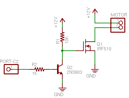
If I’d been building the circuit on a breadboard, I’d probably have started by plugging in components and wiring them up, because mistakes are easy to correct by unplugging and replugging. But since I was using larger components that I was going to need to solder, I didn’t want to have to change too many connections; so I started by drawing the schematic I intended to build.

(First I reread my May 2006 post about driving stepper motors with MOSFETs. They don’t use the same circuit, but I had taken the time to review my textbook and figure out how to treat MOSFETs right; and my blog isn’t just for y’all–it’s secondary storage for my own memory.)

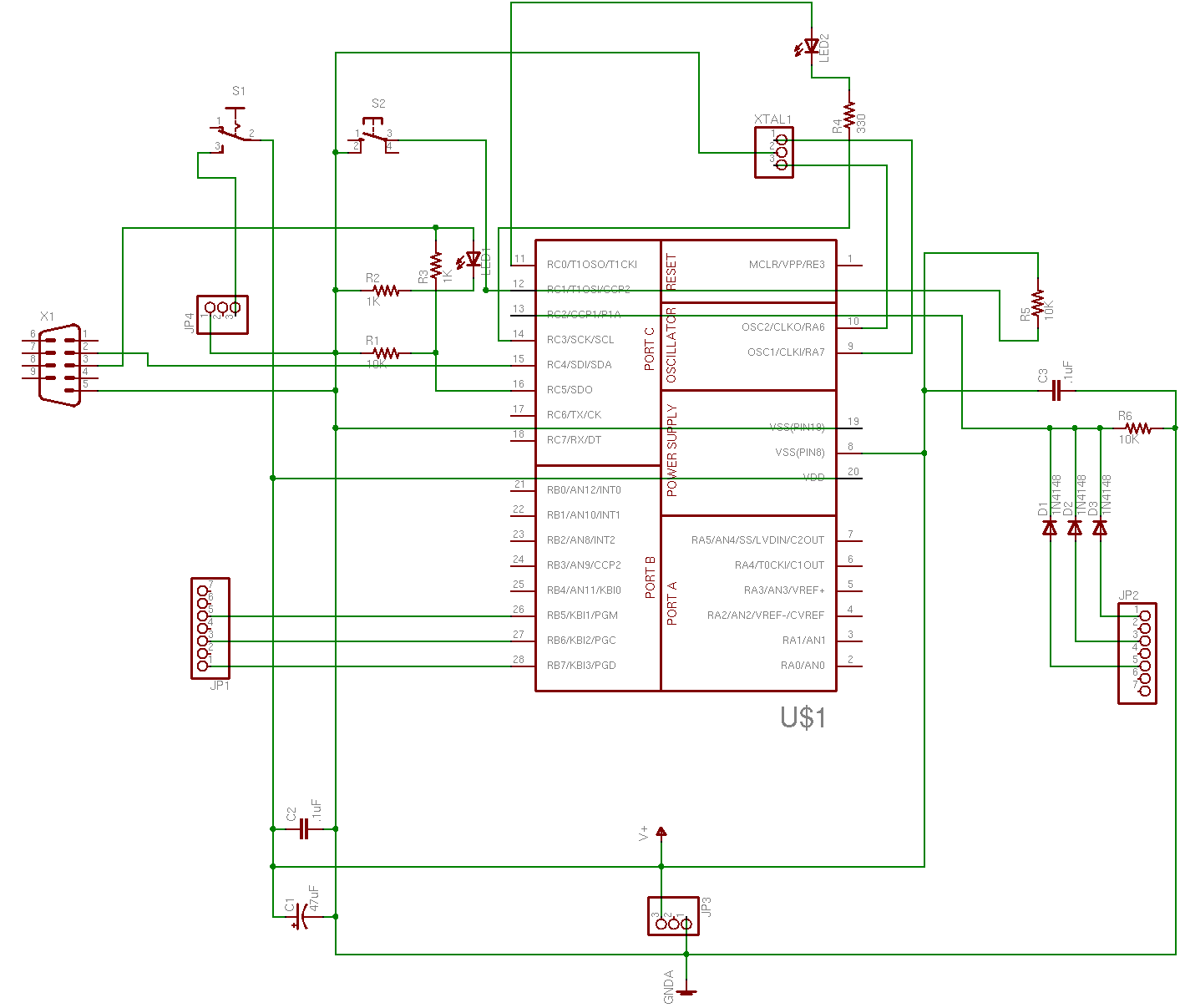
The PIC’s PWM output is on port C2. The MOSFET’s gate needs at least 7V to saturate (turn all the way on), so port C2 controls the base of an NPN transistor (any common NPN will do; I happened to have a 3903) that switches the MOSFET gate between 12V and ground. The N-channel MOSFET in turn provides a ground path to turn on the motor when the MOSFET’s gate voltage is high.

The only snag is that the bipolar transistor inverts the control logic; so when C2 is high, the motor is off; and when C2 is low, the motor is on. Oh well. We’ll compensate in software.

Wiring it Up

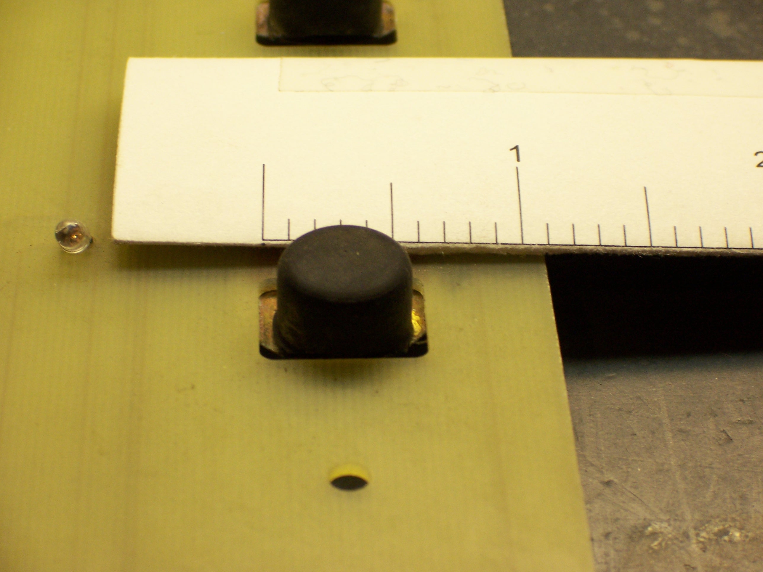
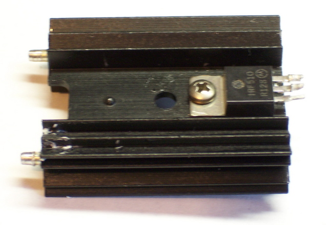
I started by bolting one of my IRF510 MOSFETs to a heatsink. I should have used thermal grease, but I didn’t have any handy and I’m doing a quick test. And I should have used an insulator (since the FET’s tab is wired to drain, and that’s not going to be ground, and the heatsink might bump into something that’s grounded), but the heatsink seems to be anodized and sorta insulated already and I’m just doing a quick test.

MOSFET mounted to heatsink

I could have used the cordless drill’s battery to power the motor, but I didn’t feel like rewiring that much of the drill right now. So I settled on using my trusty old PC power supply–and I desoldered a connector from a dead CD-ROM drive to mate with the power supply. (Bench vise, heat gun, and pliers.)

Molex power connector on CD-ROM drive board

I wired the MOSFET to the power connector and left fly wires to go to the motor and the LogoChip. As always, I put heat-shrink tubing on each solder joint to be safe. The 10K pull-up resistor at the end of the blue wire, hidden behind the yellow wire next to the power connector.

Fully-wired MOSFET and power connector

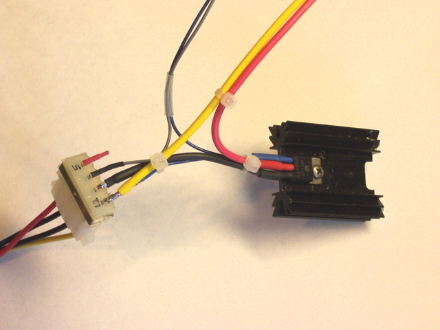
The 5V supply on the power plug isn’t needed, so I insulated it as well.

Connecting the Drill

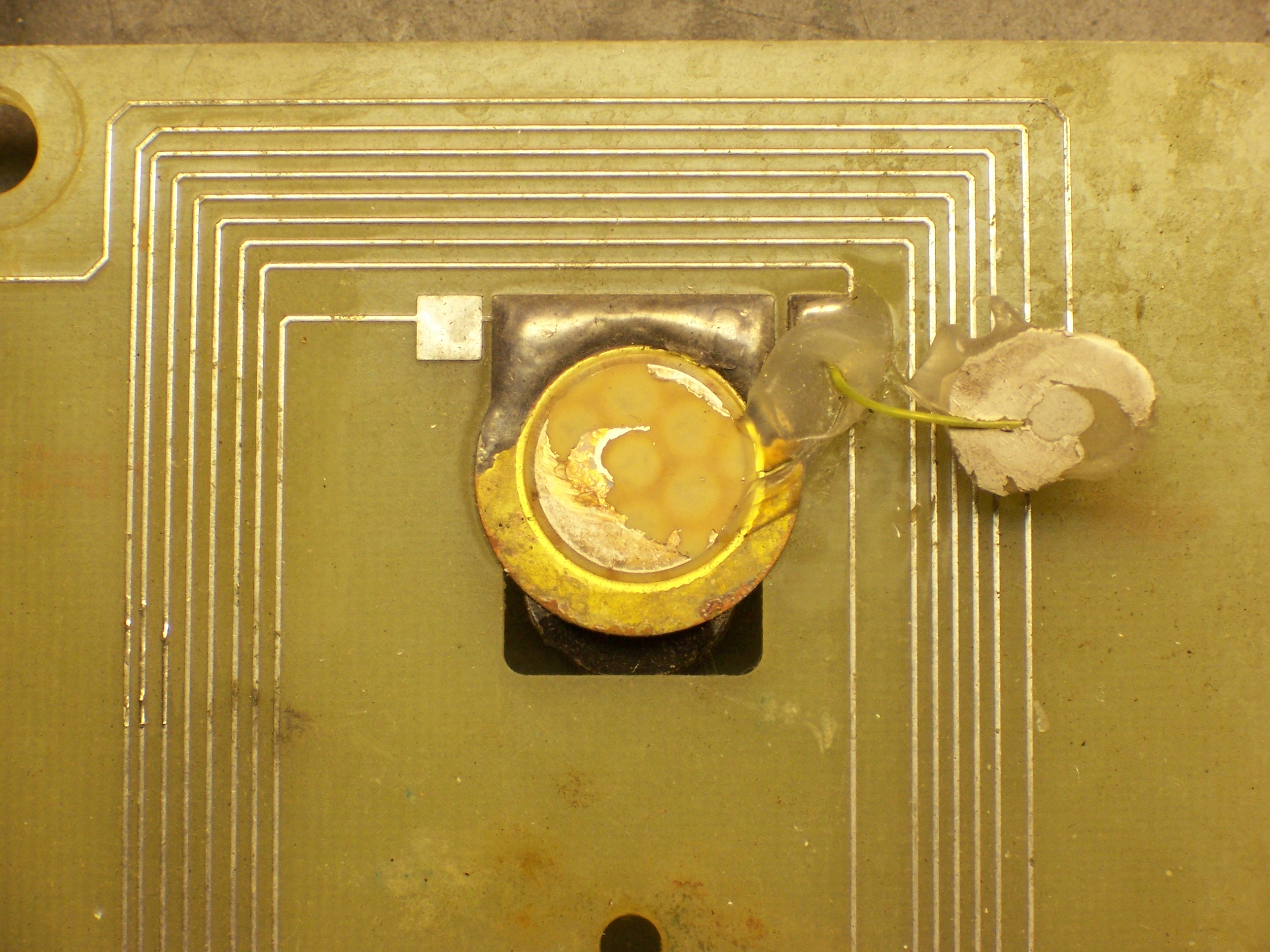
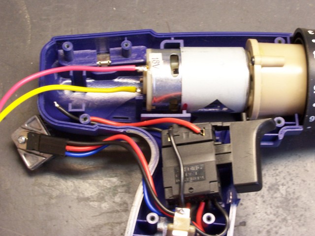
The largest DC motor that I could think of having at home was the cordless drill. It’s not as big as the windshield wiper motor that Team Doccia might be using, but it’s the best I could do. Here’s the victim with its the case removed:

Cordless drill, case opened

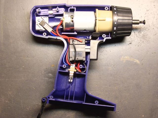
The motor is the silver and white cylinder in the center of the top of the picture. The tan cylinder to its right is the planetary gear system that reduces speed and increases torque.

To the left of the motor, you can see the MTP15N06V MOSFET that normally runs the drill. I could have reused it, but (1) then I’d have been done before I even started; and (2) I wanted to test with a FET that I had lots of, so someone else could use exactly the same circuit. Both the drill’s MTP15N06V and my IRF510 have a built-in reverse-biased diode to shunt the back-EMF spike that occurs when the supply voltage is removed from an inductive load (like a motor).

Cordless drill motor rewired for MOSFET speed controller

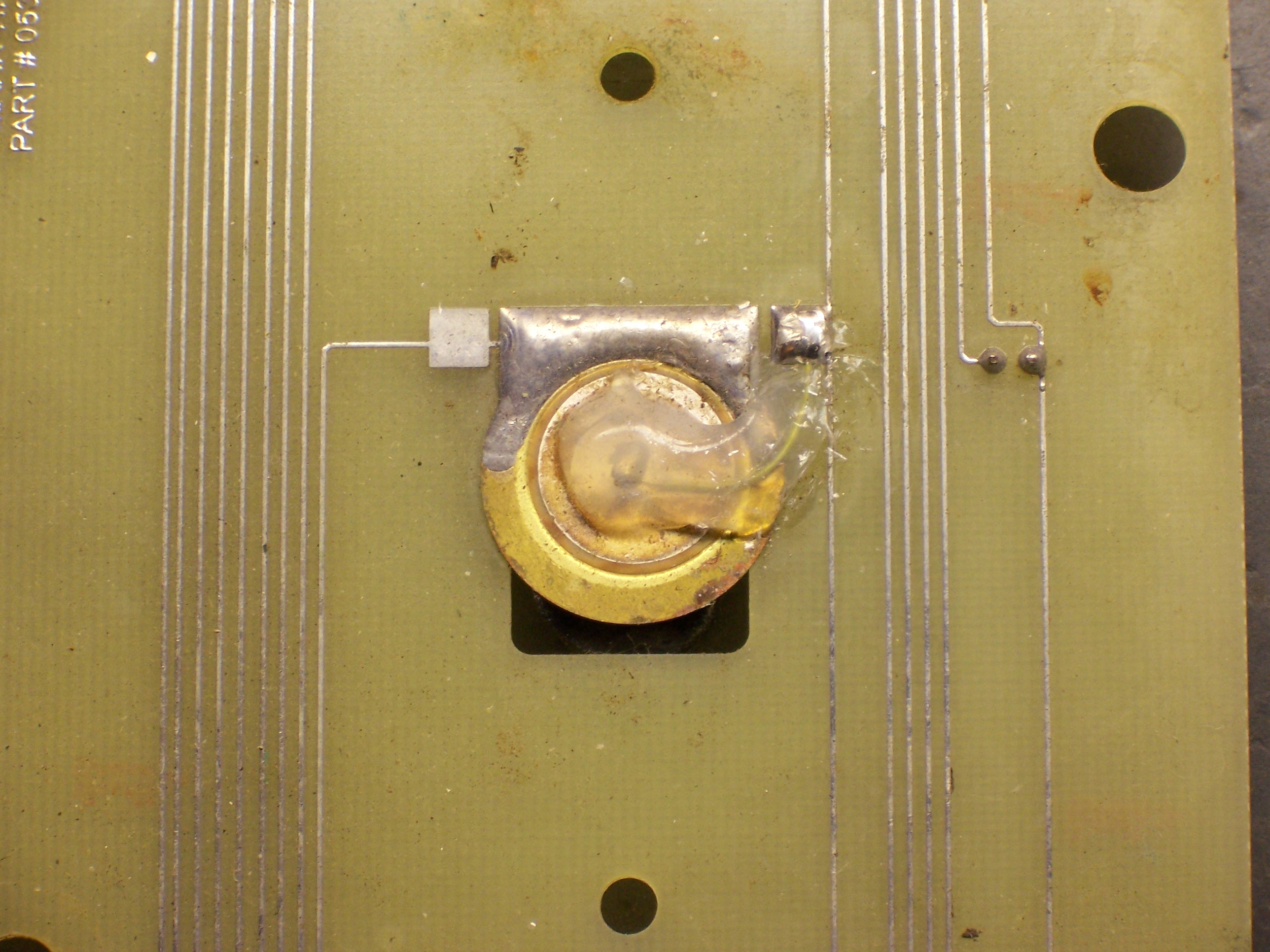
I pulled the the motor out of the drill casing, soldered on the leads from the FET wiring harness, and jammed it back in. I could have laid in on my bench for testing, but I was afraid the counter-torque when the motor started up at high speed might roll it right off the edge. The gearbox has a tab on the bottom that mates with the case and keeps it from twisting.

LogoChip Wiring

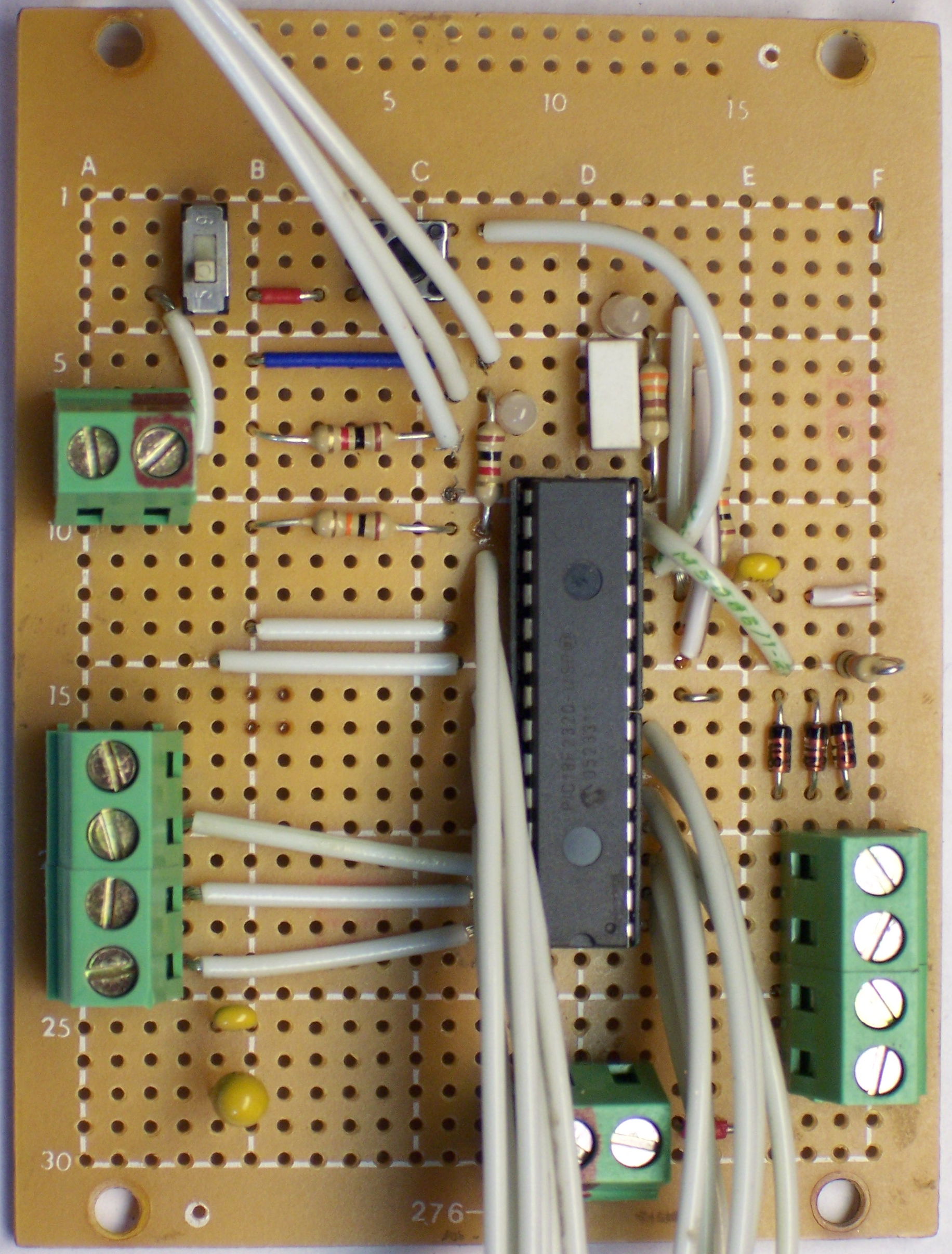
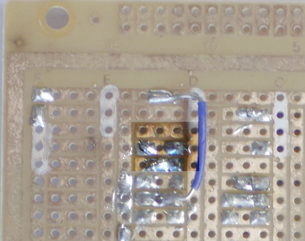
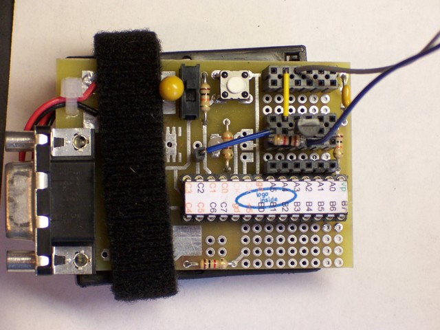
Tom left a nice prototyping area on the LogoBoard when he designed it, so I built the rest of the circuit there. I soldered a header socket into the connector for pin C2, plugged the NPN transistor into the breadboard section, and plugged in the base resistor and the gate and ground leads from the FET assembly.

LogoChip NPN switching circuit

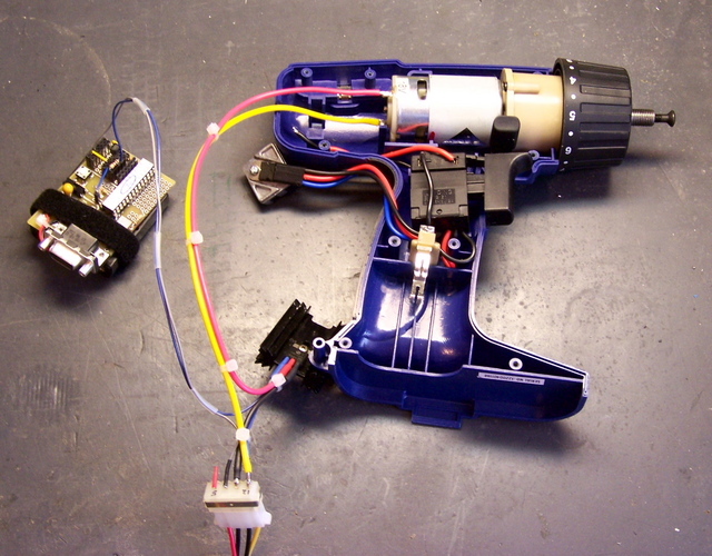
Here’s what the whole works looks like when it’s all hooked up:

Cordless drill motor wired to MOSFET speed controller

Control Software

For prototyping, I reused my old motor-pwm-demo.txt program, even though it has some extra stuff that’s not needed here. I called pwm-init and then pwm-set 255 255 to shut the motor off. (Remember, it’s backwards logic because of the inverting effect of the NPN switching transistor.) pwm-set 255 0 turned the motor on at full speed, and pwm-set 255 128 selected a medium speed. pwm-set 255 196 was about as slow as it could reliably go.

To explain the code, the first parameter (the one that I’m always calling with 255) is the period of the control pulse–the higher the number, the longer between consecutive pulses (i.e. the slower the pulse train). The second parameter is the pulse width–how long each pulse output should be on. So pwm-set 128 64 should have about the same effect as pwm-set 255 128, only twice as fast (half as long).

Unfortunately, that ain’t quite so. Due to the inductive effects of the motor coils, some frequencies of PWM control work better (more efficiently) than others. In this case, the lower control frequency is more efficient–the motor runs a little faster at 255/128 (longer pulse = lower speed) than at 128/64 (shorter pulse = higher speed).

Worse, the motor would probably like it even better if the control frequency were even lower. But I can’t do that–I’m already running the PWM clock at its lowest speed and dividing that speed as far down as it goes. This is as good as it gets.

Final Thoughts

Motor On at Powerup

When the circuit powers on, port C2 is set as an input, so the MOSFET’s pull-up resistor pulls the line high and the motor turns on at full speed. That’s bad; you never want mechanical systems initiating motion before the control systems come online.

The circuit should really be redesigned to use non-inverting buffers to get around this problem. But for now, at a minimum, the motor should be turned off in the LogoChip’s powerup routine:

to powerup
pwm-init
pwm-set 255 255
end

Operating Temperature

With an ambient temperature of 72°F, the FET got up to about 96°F after running for a few minutes. The FET is rated for 250°C and its rated capacity only drops from 5.6A at 25°C to 4A at 100°C, so it’s well within safe operating conditions. If a larger load were required, I might look at using more FETs in parallel. (I don’t even remember whether you can do that, so I’d start with the Malvino textbook and review whether parallel FETs are subject to thermal runaway.)

Low Torque

The drill really doesn’t have much torque using this driver at low speeds. Granted, the drill is rated for 18V and I was running it 12V. But I was hoping to get away with using open-loop control for robotics, and it looks like I’ll probably have to put optical encoders on the wheels to make sure they’re really turning as fast as I told them to.

I’m still optimistic that a windshield wiper motor is geared down enough, and natively runs at a low enough speed, that this control method will be adequate for Team Doccia’s breathing mechanism.

Making Googly Eyes, Part 1: Reverse Engineering

Monday, April 2nd, 2007

Back in mid-February, I wanted to demonstrate motor control with the LogoChip to class, but it’s hard to see what a motor is doing unless it’s geared down and attached to something. I decided to make googly eyes that could look around, and here’s how I went about it.

Motorized googly eyes

CD Read Sled

Although the motion of each individual eye is rotary (right to left; these can’t look up and down), to synchronize their actions, I needed linear motion.

Digression: Predator species have eyes on the front of their face, to triangulate the distance to their target. Prey have eyes on the sides of their heads, to keep the widest possible view of their surroundings and watch out for predators. Predators’ eyes generally move in synchronization. Of course, they may look slightly inward when watching a nearby object (binocular convergence; think of looking cross-eyed at your nose); but for a simple model like this, two eyes always looking in exactly the same direction is adequate.

I figured my best shot was something from a dead CD-ROM drive, so I went down to examine my stash. What I call the read sled assemblies looked the most promising–they’re the ones that move the read head in and out along the radius of the disc to find the right position to play. The tray motors might also work, but the trays have a good 5″ range of motion. The ∼2″ range of the read sled seemed much more useful.

Several of the assemblies I examined used a stepper motor, but I wanted to demonstrate a simple DC motor, so I kept looking. Finally I came across this one, which had a DC motor (on the underside), a nice geartrain, and an optical encoder (the faint grey circle between the green PCB and the medium black gear) to determine the position of the sled.

CD-ROM drive read sled assembly

The motor was mounted from the back side, and the optical disk was press-fitted to its shaft.

CD-ROM drive read sled assembly, reverse

Reverse-Engineering the Optical Assembly

I was interested in trying to reuse the optical assembly so that I too (well, my program) would know where the sled was, so I desoldered the flex pcb ribbon cable and set about figuring out the connections on the PC board.

Optointerruptor and interface PCB

The larger black rectangle that overlaps the optical disk was obviously an optointerruptor–one side has an LED and the other side some kind of optical sensor. When a hole in the disk passes between them, light is transmitted; when a bar passes between, the light is interrupted, and the receiver can tell the difference.

The two smaller black rectangles (southwest of the screw head) are surface-mount resistors, reading “181″ (180Ω) and “752″ (7.5KΩ). I could visually follow some of the traces (the light green lines) on the board, but I got lost with exactly what happens underneath the resistors.

I assigned numbers to the five solder pads from the cable, arbitrarily numbering from the outer edge of the board. (In retrospect, that was incorrect–the pad to the left in this photo is shaped differently than the others; that makes it pin number 1. Ah well.) Then I made this table (actually edited here on my blog–all the notes have been sitting around for six weeks, and it’s only the narrative that I’m adding later) describing where each pin went, to the best of my visual acuity.

Pin Connection
1 motor black wire
2 motor red wire
3 interruptor
4 interruptor end of 7.5KΩ resistor
5 both resistors

Pins 1 and 2 obviously run to the motor, and it was pretty clear that they didn’t have any connections to pins 3-5. So I used my ohmmeter to measure the resistance in each direction between each pair of pins out of 3-5. I got this:

4 → 3: 50KΩ
3 → 4: ∞
5 → 3: 40KΩ
3 → 5: ∞
5 → 4: 7.5KΩ
4 → 5: 7.5KΩ

It was obvious that pins 4 and 5 were connected directly via the 7.5KΩ resistor. It was also apparent that there were diodes from pin 4 to 3 and from pin 5 to 3. That gave rise to this diagram:

CD read sled connection diagram, reverse-engineered

Which made a lot more sense once I redrew it like this:

CD read sled connection diagram, redrawn

Pin 5 is the supply voltage, pin 3 the ground, and pin 4 the readout of the voltage divider between the 7.5KΩ resistor and the photosensitive diode. Voila!

Using the Optical Encoder

A 180Ω current-limiting resistor with a 5V supply would give ∼24mA of current through the LED, and that seemed a little high. I’m guessing that part of the circuit ran on 3.3V, making the LED current ∼14mA–a more reasonable value.

I wanted to shoot for 15mA, so 4.3V / 15mA ≅ 290Ω, of which 180Ω was already in the circuit, leaving 110Ω to add. I had a 120Ω resistor in my bin, so 4.3V / (180Ω + 120Ω) ≅ 14mA, which was close enough. I used the 120Ω resistor to wire pin 5 to the 5V supply, placing it in series with both diodes. (I figured its impact on the 7.5KΩ resistor and photodiode whould be negligible.)

Turning the encoder wheel very slowly and carefully and reading the voltage at pin 4 yielded a minimum voltage of .77V and a peak of 3.4V. (Alas, I don’t remember which was when the light was blocked and which when it was passed . . . probably the photodiode conducted and pulled it down to .77V when light was passing . . . but I don’t know that I really care.)

I didn’t really want to have to use an A/D converter input and deal with a 10-bit numeric value when all I needed to know was whether the light was blocked or passing. But I wasn’t wild about feeding a continuously varying analog voltage into a TTL input–it tends to make them overheat. Happily, the PIC datasheet (p. 102) revealed that pin A4 has a Schmitt trigger input, and my problem was solved.

A Schmitt trigger has hysteresis–the input signal has to rise above a certain point (the “high-water mark”) before it reads high, then fall below a lower point (the “low-water mark”) before it reads low. It’s intended for reading digital values from analog signals, it was exactly what I needed, and it worked exactly as desired. I fed the optointerruptor signal into A4 and got clean, predictable digital results.

Next Steps

That’s probably long enough for one post. Next: Building the eyeball assembly and programming the motor.

Piezo Elements for Percussive Input

Sunday, April 1st, 2007

Harry Partch and Piezo Instruments

Lauren Hirsh, a WSU percussion student, WSU Internet radio goddess, and all-’round CRATEL regular, is involved in a performance of Harry Partch compositions this spring. Partch composed for new instruments he created, and the percussion department is attempting to build at least one or two of them for the concert. Lauren is taking on the task of building one, I believe the boo.

The boo is a marimba-like instrument made from tuned bamboo tubes arranged in six ranks. Rather than try to reproduce the tonal qualities of the original instrument through physical means, consideration is being given to building an input interface and using electronic reproduction of the boo sounds. In other words, Lauren wants to build a synthesizer keyboard shaped like a marimba. And several of us involved in CRATEL are intrigued by the challenge.

Tom McGuire has done all the work so far. He got a piezo element and hooked it up to the LogoChip. When you strike it, it generates a voltage; he’s working on capturing the voltage in a capacitor until the LogoChip can come along and poll it. The capacitor doesn’t have a drain resistor; he’ll turn the LogoChip port into an output at 0V after he’s read it, to drain it manually. In other words, he’s making a piezoacoustic version of the CCD camera. Brilliant!

Here’s a picture Tom sent of the element attached to a PVC faux bamboo tube:

Tom McGuire's piezo element interfacing

Sources

Tom has a few piezo elements, but maybe not enough for the whole instrument (even though Lauren only wants to construct a couple of ranks). But tonight, I mentioned the situation to my friend Joel, and he rooted around to bring out four boards with a dozen piezo elements each, which he’d be happy to donate as long as they don’t all get used up.

Piezo board, back

Each piezo has a rubber-covered button stuck onto the front–Joel thinks they may have come from an ATM or some other heavy-duty input system. It doesn’t feel like they can be removed easily, and I don’t know whether that will prevent them from being useful.

Piezo element, knob on front

Worse, they’re a bit corroded, and trying to remove the silicone that holds down the wire tends to rip the foil right off the back. I don’t know if there’s enough salvageable here or not, but I wanted to post the pictures to let Tom have a look.

Piezo element, back, torn

One I haven’t torn yet:

Piezo element, back

LED Gloves

Sunday, April 1st, 2007

Background

Steve Wilson is a graduate student involved in WSU’s CRATEL (Center for Research in Art, Technology, Education, and Learning) program, and his video synthesizer was sponsored for further development in last year’s BETA (Bridging Entrepreneurship, Technology, and the Arts) competition.

One of Steve’s challenges for his video synth, and an interest in general, is creating expressive interfaces to electronic instruments. He describes it in a post to the Technology: Art and Sound by Design class mailing list. Basically, it comes down to the idea that acoustic instruments offer an immense amount of control over the sound that comes out through physical manipulation, and electronic instruments tend to offer much less control, and through mechanisms mainly like knobs and sliders.

While brainstorming with Steve about his synth, several of us came up with the idea of an interface like a plasma globe, which you control by moving your fingers over the surface. A cheap videocamera inside could watch what was happening and control the action.

Apparently a group of engineering students have been working on the globe subproject for six months without much progress to report. Although their difficulties seem to be mainly lack of organization and lack of time, others of us had talked about how clear an image might be obtainable on the camera with the globe lighted from the inside or outside.

Finally it occurred to me (while driving home from work) that gloves with LEDs on the fingertips would make lighted spots that should be very easy to see from the inside of the globe. Different colored LEDs on different fingers would allow the driver software to identify the different fingers; and pressing the LED against a translucent surface will produce a sharper point than holding it further away, so it might even be possible to determine approximately how near a fingertip is to the globe’s surface. And if made properly, the glove could be worn without impeding other use of the hand–just adding lights for the globe.

Time to prototype.

Gloves

I was hoping to find a cheap lycra glove to make something like the original Dataglove. (Yes, I have a Dataglove system. No, you can’t play with it.) What I found instead was certainly cheap, but knit cotton instead of lycra. Heck, for 96¢, it was good enough.

When I put the gloves on, I could feel that they’d been assembled somewhat sloppily. Inside-out, it was easy to see that there was a lot of extra fabric inside the fingers outside the stitching:

Fingers need to be trimmed

So I trimmed it a little closer and more evenly around the fingertips, for better fit and comfort.

Fingers trimmed

LEDs

I wanted to use surface-mount technology (SMT) LEDs, so they’d fit flat against the glove surface. The ones in my stockpile are out of broken digital office phones, used to light up beside the line appearance and feature buttons.

I wanted to be sure I knew the polarity before I started attaching things and soldering them together, so I tested first with my meter. The LEDs actually lit with the small amount of current it supplies, which was kind of cool. Curiously, the green LEDs have the anode on the end with the cut corner, and the red LEDs have the cathode on the end with the cut corner. On each LED that I identified, I marked the anode end with the color of the LED. (The ones on this sheet are tinted to indicate their color, but the ones I’d already removed weren’t.)

The phone flex-PCB has a 300Ω resistor in series with each LED, so I tried out a couple there on the strip. Nice and bright.

Testing an SMT LED

Soldering the LEDs

My plan was to solder wire the LEDs, then sew the wire through the glove to the back side, where I wanted to attach a battery holder. I got out some fine wire, scraped off the enamel insulation, wrapped it around the fly leads on the LED, and soldered it up.

Soldering the SMT LEDs

Sewing

After I had both wires soldered to the LED, I threaded one at a time through a needle, held the LED about where I thought I wanted it on the fingertip, and started sewing. The goal was to get the wire from the tip of the finger to the back of the hand without leaving any large loops that might snag on anything, and without reducing the stretchiness of the glove. The latter factor called for a zig-zag stitch, which with a single thread looks like a running pattern of slash marks.

LED on second finger

Once I got the wire stitched around to the back side, I followed along the back of the finger and then curved toward the center of the back of the hand.

Stitching from the back of the finger toward the battery

Glue for Protection

I needed something to protect the LEDs on the fingertips so they wouldn’t snag. When the wires were safely stitched around out of the way, I got out the hot glue gun, put on the glove, put a dot of molten glue over the LED, and pressed the glue into a perfectly-shaped dimple in a USB serial connecter that I lifted from the CRATEL lab. It soaked into the fabric a bit, adhered very well, and made a nice smooth bubble over the LED.

Glue bubble over LED

Well, mostly nice and smooth. Hot glue tends to stretch like pizza cheese, and I made a little boo-boo.

Battery Holder

For now, I settled on prototyping just two fingers, because I have only two colors of SMT LEDs, and because it seemed like enough for a proof of concept. I steered the appropriate wires onto the same paths and ran them up to where I wanted the battery holder.

Back-side stitching for two fingers

Then I clipped the wires short, scraped the ends, folded the glove over to get room to work, and wrapped the wires around the leads of a surface-mount coin-cell holder salvaged from a PC motherboard.

Soldering battery holder

I soldered them on, then folded the battery holder leads underneath so they wouldn’t poke through the glove and scratch up the hand. Laid back out, it looked like this.

Back of glove with battery holder attached

The Lights

I didn’t bother with a switch on the prototype–just pop in the coin cell and the LEDs come on. And because I’m using an old, small battery, I didn’t bother with current-limiting resistors–the internal resistance of the battery seems to be enough to limit the current to the LEDs.

Lighted fingers

Due to the idiosyncracies of my digital camera, the green LED on the index finger doesn’t look very green in this picture, but it really is. It’s a lot dimmer than the red LED, though; and I’m not sure why that is. Before going beyond a prototype, I’d want to pick current-limiting resistors to more closely calibrate the brightness of the different LEDs.

I don’t have a translucent globe to use, but I borrowed a hemispherical Tupperware bowl from my friend Lawrence’s daughters. (Don’t ask my why the girls have their own set of Tupperware–I really don’t know.) It works well enough to demonstrate the idea:

LED fingers through Tupperware

You can clearly see where the red LED is touching the bowl. Now all we need is a videocamera, some fancy software to track the lights, and an interface to a video synth. :-)

Seriously, all of those things are Steve’s domain. I just wanted to see whether I could throw together a working glove, and I think this’ll do.

Oh–and when you want to shut it off, you take out the battery and drop it into the thumb.

LogoChip Port A, setbit/clearbit, and analog inputs

Friday, February 16th, 2007

Twice before, I’ve run into problems with the lines on the LogoChip’s port A not working the way I expected–while programming an interface to the A6276 LED driver, and again when trying to interface to the DS1302 real-time clock. The second time I ran into it, I fixed the problem by changing port A out of analog input mode–but didn’t know why that made a difference. Last week, poring over the PIC18F2320 datasheet, I finally figured out what’s going on and why the analog input mode matters.

I was working on output routines for TASD’s Thing 3: Simple Outputs, and we’re using port A because it’s the most conveniently placed on the LogoBoard. Every time I’d do a setbit or clearbit command against a line on port A, all the other outputs would change to 0.

Tom McGuire had run into this problem recently, and worked around it by reading and writing the port A latch, LATA, instead of the port register itself. But that still didn’t explain why it was happening in the first place. So I sat down with the datasheet and looked at the port operation diagrams.

Generic I/O Port

PIC18F2320 datasheet, Figure 10-1

Here’s the diagram for a generic I/O port, from page 103 of the datasheet. Writing to the port or latch register (WR LAT or Port) puts data into the data latch, which is accessible by reading the latch (RD LAT) register. Additionally, when the data direction latch (TRIS latch) is in output mode, the data latch drives the I/O pin for output. Finally, the input buffer continually reads the I/O pin (even when outputting) and makes its current state accessible by reading the port register (RD Port).

So you can always write output data to the port or latch register; and when the port is in output mode, the last data written will be output to the pin. The last data written is always readable from the latch register; and when in output mode, the data is also readable from the port register.

Port A

Now look at port A, from page 103:

PIC18F2320 datasheet, Figure 10-2

The most visible difference is that the simple output buffer from the data latch to the I/O pin has been replaced by an arrangment of an OR gate, an AND gate, and N- and P-channel FETs. As far as I can tell, there’s no operational difference between the two–Figure 10-2 simply shows what’s happening in more detail.

More significant is the addition of the Analog Input Mode line controlling the input buffer–this is the crux of my problem. When port A pins are receiving analog input, it doesn’t make sense to feed that input into a TTL register–in fact, it could cause excessive power draw and overheating. So the input signal is gated by the analog input mode before feeding to the port A read line (RD PORTA).

setbit and clearbit

The reason this matters is that the LogoChip’s setbit and clearbit commands are read-modify-write operators–they read the value of their target, OR or AND that value with a constant, and write it back to the target. When that target is the port A latch register, all works as it should–the latch is read directly back out the RD LATA line.

When the target is the port A data register, however, the current value is read through the input buffer, which is gated by the analog input mode line. When the pin is set in analog input mode, even though the data direction is set to output, the port data cannot be read because the gate is off, and always returns a 0.

So when setbit <bit> porta attempts to change one bit, it tries to read PORTA and returns %00000000 rather than the value of the data latch. It then sets one bit and writes the new (mostly-cleared) byte back out to the port A data latch–clearing every other bit of port A in the process.

Workarounds and Solution

Two workarounds are obvious. Tom’s method was to manipulate the port A latch (LATA) instead of the port A data register (PORTA). The latch can always be read and written directly, so this works flawlessly. My only objection is that porta is already defined as a constant in LogoChip Logo. I’m not wild about having to teach students to define a new constant for lata and then use lata, portb, and portc.

The second workaround is also simple. When using the LogoChip setbit and clearbit commands, clear the analog input mode on any pin you want to use as an output. Because the order of analog input pins is predetermined (A0, A1, A2, A3, A5, . . .), this might mean rearranging the pinouts–you can no longer have A0 and A2 as analog inputs and A1 as an output, for example. But it’s a pretty easy method.

The true fix is equally simple. Where port A’s TTL input buffer is gated by (active-low) analog input mode, it should in fact by gated by (active-low) analog input mode OR (TRIS Latch is set for output). That is, any time the pin is NOT in analog input mode, OR the pin is set for output, pass the pin’s value to the port data read buffer. I don’t see any drawbacks to this solution, other than the cost of one additional OR gate.

Having taken the time to figure that out, I’m rather surprised that Microchip didn’t build the PIC that way.

LogoBoard

Monday, January 29th, 2007

Well, it’s time for another round of John Harrison’s Technology: Art and Sound by Design class–and oh by the way, this time I’m co-teaching. John’s doing the hard parts (course vision, blogs, wikis, etc.), and I’m doing the technology lessons for a while.

We’re calling them “Thing a Week,” sort of like another Thing a Week series you might have heard of, only different. On Monday and/or Wednesday, we introduce a technical topic, Friday we build it in the lab, and then next Monday we show it off.

So here’s the first one–me soldering up a LogoBoard, a carrier board for the LogoChip, designed by Tom McGuire.

Thing 1: LogoBoard Assembly (may move to here)

LogoBoard

Funny how a 15-minute soldering job turns into two and a half hours when you stop after every part to take pictures. :-)

Arduino Circuits and Tutorial

Sunday, October 15th, 2006

Tod Kurt is posting lecture notes from an Arduino class on his blog. It’s Halloween themed, and the two sets of notes posted so far look like a really nice introduction to electronics and the Arduino. Go, Tod!