Arduino First Impressions

August 12th, 2007 by Keith Neufeld

I’m back to working on my CNC machine and wanted to hook some joysticks up to a microcontroller to run the motors back and forth during development, before I have the whole thing running under computer control. I realized that the PIC18F232 (LogoChip) has only two PWM outputs and I have three motors to control, so the LogoChip isn’t going to be ideal for this.

The Atmel has scads of PWM outputs, so I finally busted out the Arduino I bought a year ago from SparkFun Electronics. The Arduino is, to snip from their own description, an open-source prototyping platform based on a couple of Atmel microcontrollers.

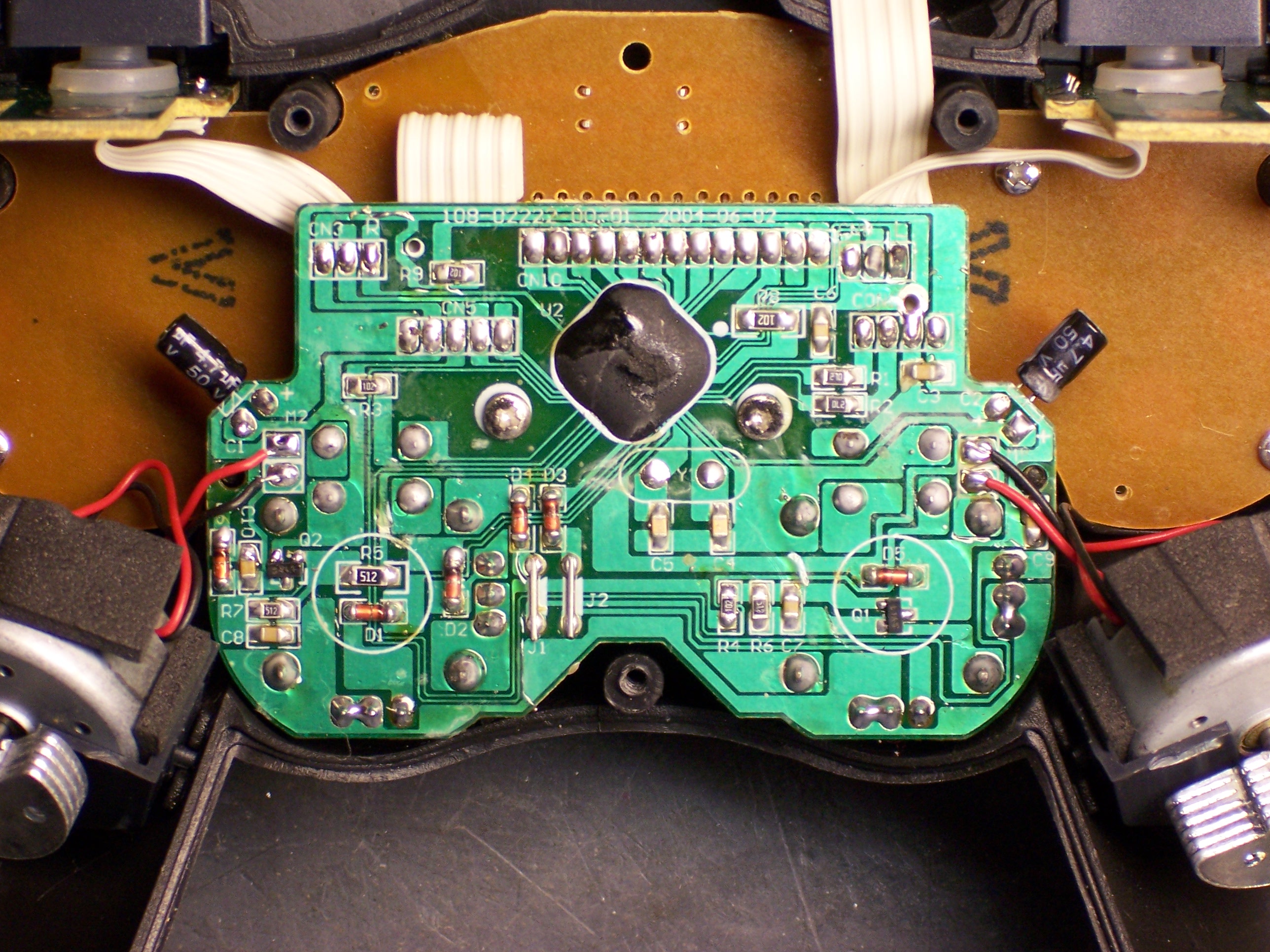
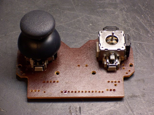
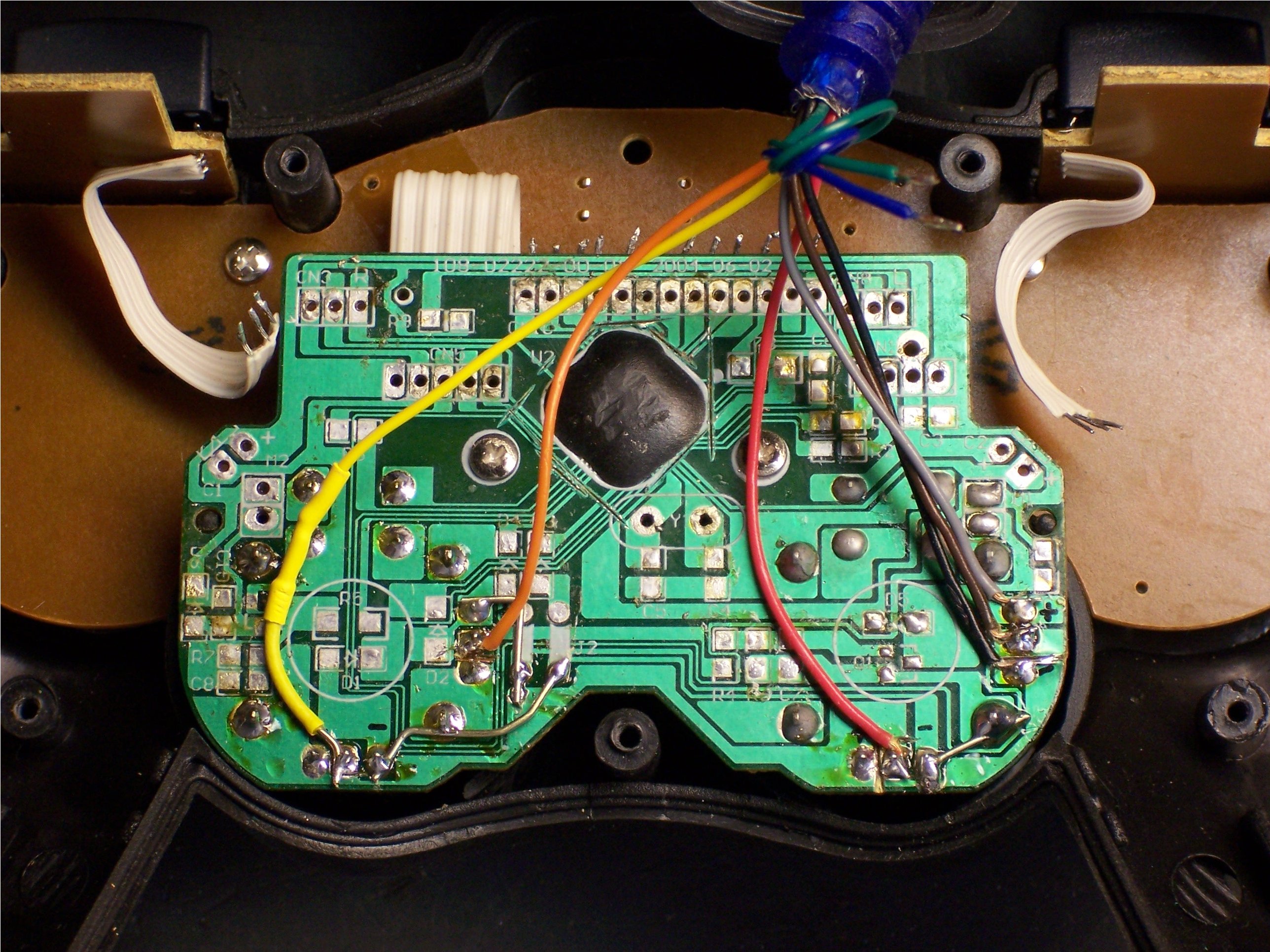
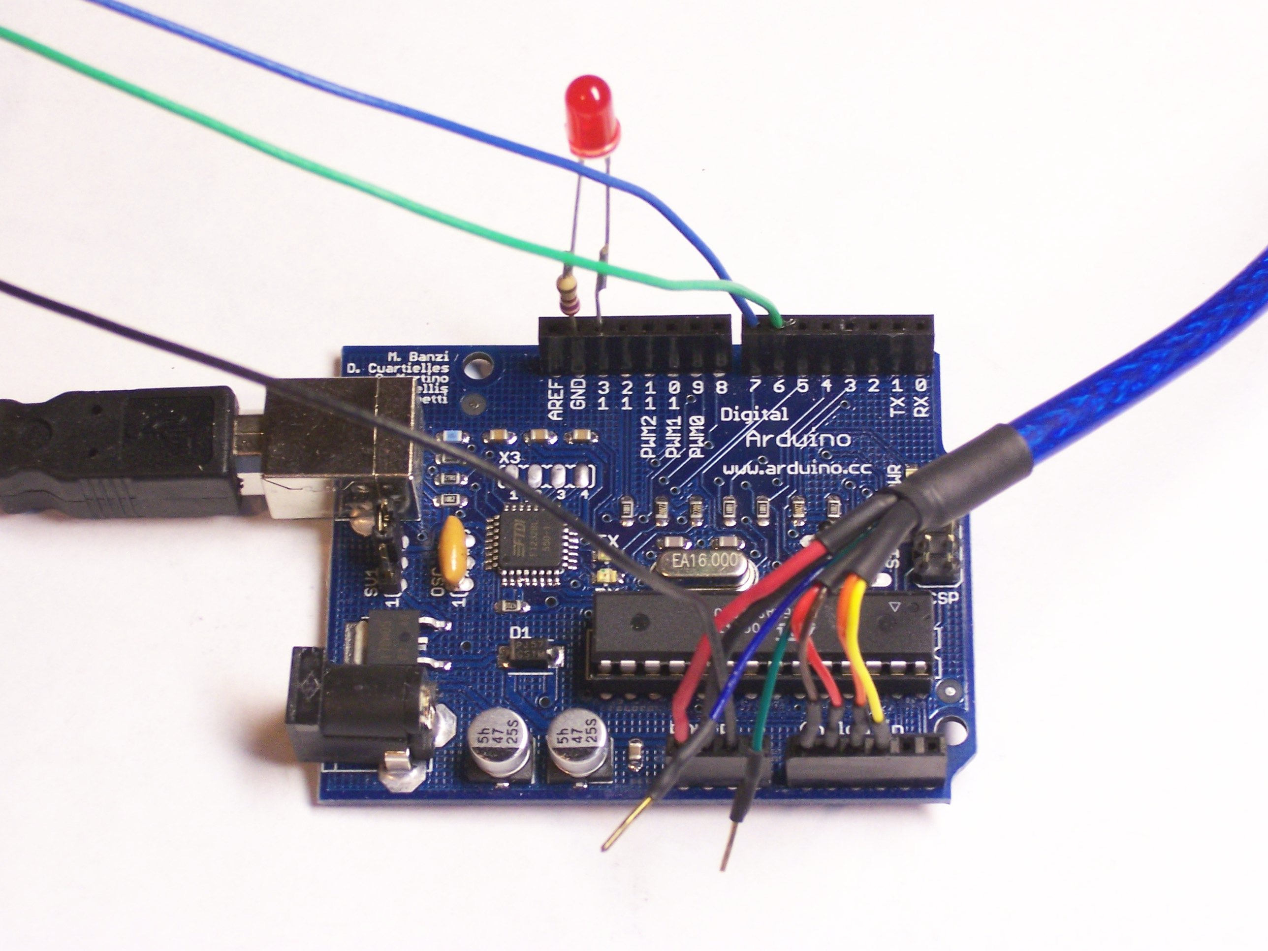
Arduino with joystick, LED, and stepper controller attached

The Arduino folks really shined up their Macintosh dev system install procedures since the last time I looked — I downloaded a zip file, double-clicked a USB driver installer and rebooted, double-clicked the IDE icon, and I was in.

I played with the Arduino Friday night. It’s really, REALLY nice to be programming in C again. I had come to the conclusion earlier from looking at the language that it was C with some microcontroller-specific libraries provided, and that’s exactly what it is. The documentation even mentions that it’s using avr-gcc underneath.

Here are my first impressions:

  • The early Arduino board I have requires you to press the reset button each time you want to download code. This is a huge pain. The newest boards have reset magic built into the USB circuit.
  • It waits about seven seconds after power-up or reset to see if you’re going to download new code to it before it starts running your program. That’s a long delay waiting for something to happen, especially if you’re not even connected to it. I expect that could be shortened by tweaking the bootloader, but I suspect you’d need a real Atmega programmer for that.
  • Taking power from the USB port is really cool, particularly during the development phase when you’re constantly tethered anyway.
  • I don’t like the GUI-based text editor in the integrated environment — but then I never do. I understand there’s a way to do all this stuff from the command-line (so advanced developers could edit with vi or emacs), but I haven’t looked up how to do that yet. (Remember, first impressions.)
  • PWM frequency is fixed by the firmware. There’s example code to change it, but the frequency is probably controlled directly by a hardware timer, and I don’t know if there are enough timers to run three PWMs at different frequencies. So the Arduino may not be any better for this application than the LogoChip was. :-)

So overall, it’s super easy and fun for geeks with programming experience. Proooobably not a good introduction to microcontrollers for visual arts students, though.

Auto Power Sequencer for SAE A502 and A202 Amplifiers

August 7th, 2007 by Keith Neufeld

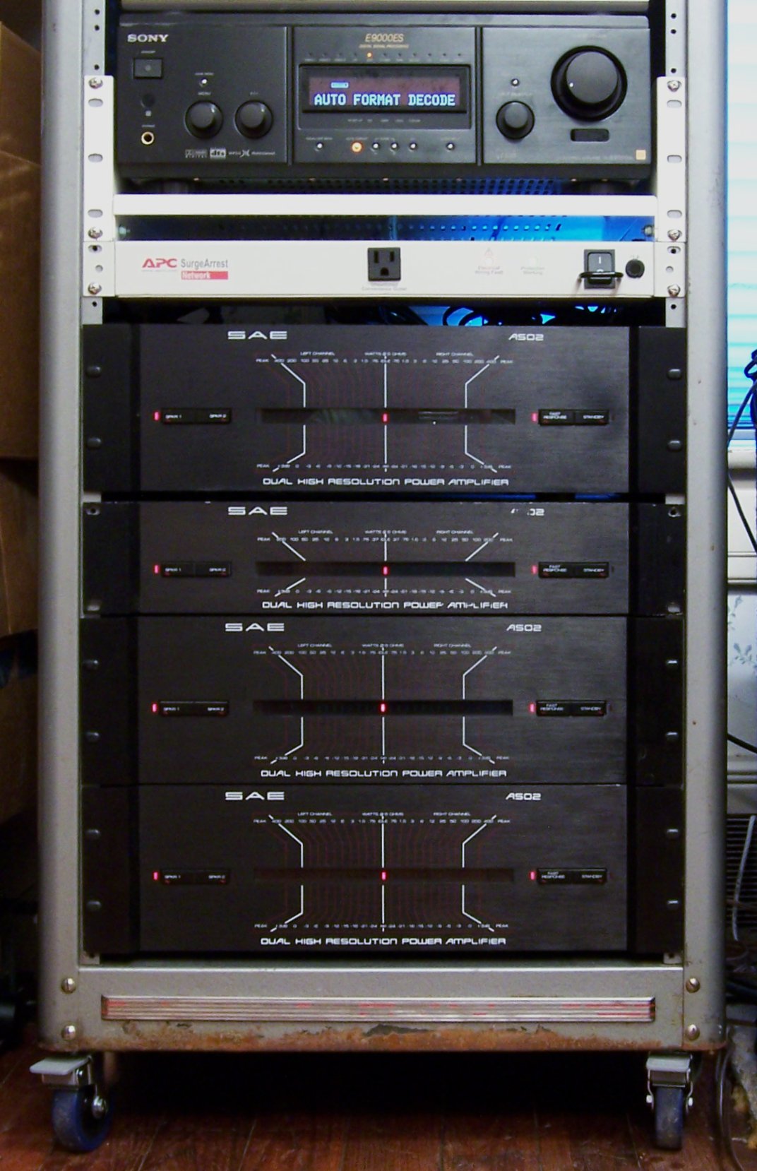
The project I’ve been working on lately is a power sequencer for my SAE A502 and A202 amplifiers. I bought my first A502 with summer job money when I was in college, and recently I’ve bought a few more on eBay. They’re big and beefy and I love ‘em.

My stereo rack, with Sony preamp and SAE amplifier stack

Their only drawback is that they have to be switched on and off manually — they’re not tied to my preamp. This is particularly annoying to my wife who hates all things electronic — she just wants to watch TV or a movie, and she has to fiddle with all these buttons to get the sound to come on.

Well, not any more.

Standby Circuit

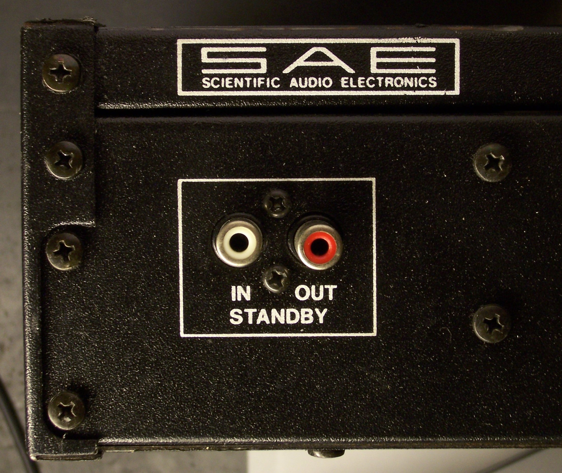
Many of the SAE amplifiers, particularly including the “02″ series, have standby inputs. The SAE preamplifier puts out a signal telling the amplifiers when to turn on and off, and the whole stack is controlled by the preamp.

SAE amplifier standby input

Which is great if you have an SAE preamp and you just want to listen to stereo audio — but SAE went out of business long before the advent of home theater surround sound, much less 5.1 surround. If you want surround, you’re not using an SAE preamp; and if you’re not using an SAE preamp, you’re turning your amplifiers on and off by hand.

I’ve long dreamed of building a box to do that for me, and now I’ve done it.

The first step was determining how the standby signalling is done. The owner’s manual isn’t much help; it doesn’t list the details of the protocol, but only describes (in rather roundabout language) that you need to manually turn the amp on and let the preamp turn it off.

So I opened an amplifier and looked at its standby board. The circuitry is very simple, and I’ve since confirmed my schematic against the amplifier’s official schematic.

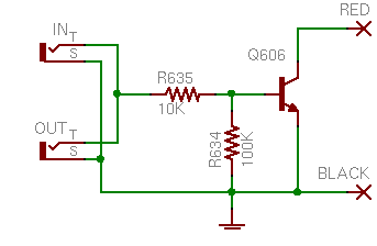
SAE amplifier standby circuit

The “input” and “output” jacks are identical and tied directly together, with the tips feeding the base of an NPN transistor. Put a small amount of current through the tip and the transistor will shunt the red wire’s voltage to ground.

Inside the amp, the red wire connects to the base of a Darlington pair that drives the main power relay. Steal its base current and the relay can’t switch the main power on; hence the standby is an override to keep the amp off, as the manual described.

Knowing that, it’s very simple to build a device to control the amplifiers.

Watching the Preamp

The question that remains is how to know when it’s time to turn on. In my case, since I have an A/V preamp, I thought the preamp put out a video signal any time it was on (even if it was just a bluescreen when no inputs are active). It turns out I was wrong, but this was still a productive train of thought.

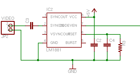
I used an LM1881 video sync separator chip to watch a video connection. The chip ends up generating sync signals if none are present, so I couldn’t use its sync outputs to detect the presence of video; but it has a logic-level odd/even frame output that oscillates at 30Hz whenever an interlaced video signal is being received. Repeated rising (or falling) edges == video present.

LM1881 video detection circuit

I had already built and tested the circuit before I discovered that my preamp most certainly does not output video when it’s on, unless it actually has a video input on as well. That was very disappointing, since I don’t want the system dependent on a third device that supplies video — it should work whether I’m watching a movie, listening to a CD, or listening to 8-track.

Skulking around for alternatives, the best I could come up with was the switched outlet on the back of my preamp. I bought a slim 5V wall wart to plug into the back of the preamp and added another detection circuit to rectify and regulate an arbitrary low-voltage input.

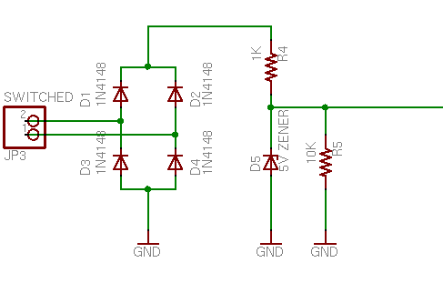
Switched power detection circuit

The preamp powers up, the switched recep comes on, 5V feeds into the bridge rectifier, and a logic high feeds out. The input would do just as well detecting a low-voltage AC wall wart . . . if I had remembered to put a capacitor between the diode bridge and R4. Duly noted for the next version.

Control Logic

Cort was saying that I should have built the whole circuit out of discrete TTL logic, and I could indeed have done so, for a little retro charm. However, I wanted additional control that would have raised my chip count too high, so I built the control with a PIC.

When the preamp comes on, the sequencer turns on all four amps, one at a time, to spread out the inrush current. (Could have used a clock and a shift register.) But all four amps are only needed when watching movies — listening to music requires only the front and sub channels, not the center and rear. I wanted manual override pushbuttons so I could turn off the unused amps. (Could have used S-R latches.)

Additionally, when Cort and I were discussing what should happen to manual selections when the preamp eventually turns off, he suggested having a fully manual mode that ignores the signal detector inputs and heeds only the front-panel pushbuttons. (Could have . . . naahhhhh.)

Ultimately, I ended up using every available I/O pin on my PIC18F232:

  • 1 capture/compare input pin to watch the video signal
  • 1 input pin to watch the switched power signal
  • 2 output pins to run the bicolor power/mode LED
  • 4 input pins to watch the front-panel pushbuttons
  • 4 I/O pins to run bicolor amplifier status LEDs using the tristate trick
  • 4 output pins to control the amplifier standby inputs

I wrote the code in LogoChip Logo, with subroutines to service the input modules and a state machine to control the different modes. All of the timing is done in software, including the delay between turning on consecutive amps, and a loss-of-video countdown timer to keep short glitches from bouncing the amps.

Sequencer in Action

The video detector wasn’t a waste; I plugged a spare output of my DVD player into it, so the amps come on when the DVD player is turned on or the preamp is turned on, whichever comes first.

Here’s a video of me turning on the DVD player and the sequencer (just above the amp stack) turning on the amps, then turning off the DVD player and the sequencer turns off the amps after a delay. If you have audio turned on, you can hear the amps’ relays clicking in sync with the sequencer LEDs, then later clicks as the delayed speaker relays engage.

This is really slow to load; I’m working on migrating this to YouTube.

These are too slow to load and are causing problems with my browser. You’re welcome to paste in the URL and try them if you like.

embed src=”http://www2.neufeld.newton.ks.us/images/electronics/2007/08/06/100_3046.mov” controller=”true” width=”480″ height=”656″ kioskmode=”false” autoplay=”false” pluginspage=”http://www.apple.com/quicktime/download/”>

There’s one little snag — the standby circuit on my top amplifier isn’t working, so I’m still turning it on and off manually. I just bought an SAE preamp on eBay and should receive it within a week or so, at which point I’ll hook it up and see whether it has magic juju that my sequencer doesn’t, or whether I need to troubleshoot my amp.

Here’s a nearly identical video of me turning on the preamp and the sequencer turning on the amps.

embed src=”http://www2.neufeld.newton.ks.us/images/electronics/2007/08/06/100_3047.mov” controller=”true” width=”480″ height=”656″ kioskmode=”false” autoplay=”false” pluginspage=”http://www.apple.com/quicktime/download/”>

Kits for Sale

Well, not yet, but I’m interested in pursuing it. There’s a pretty active community of SAE equipment owners, and I have to believe there’d be other folks in the same position, using SAE amps with non-SAE preamps. After I work through a few issues, I’d like to offer the power sequencer in both kit and appliance form and see if I can sell a few.

I want to split the main circuit board into a front-panel board and a control board, to make it easier for other folks to adapt the LED and button spacing to fit enclosures of their own choice. That also solves the problem with the RJ-45 jack, as it could then be on the component side of the control daughterboard. And I made some mistakes in the physical size and mounting of the board that I’d like to correct as well.

Once I touch up the circuit and board designs and clean up my code, I want to release the whole schmear under a Creative Commons license, probably Attribution Share Alike. Lady Ada’s Creative-Commons-licensed kits are pretty inspiring to me, and I’d like to think there’s a small but healthy market for kits and appliances that don’t rely on keeping the design closed and secret.

Wish me luck!

PCB Iron-On Etch Resist Problems (and Solutions)

August 6th, 2007 by Keith Neufeld

After drilling my board (and finally getting the right holes in the right order), I took it back home to etch. I wanted to print an etch-resist mask on my laser printer and iron it onto the board, and I wanted to do it using plain, glossy paper.

Pads and Holes

I had originally laid out the board using default sizes of 28 mil holes and 50 mil pads. Since I broke too many drill bits and ended up drilling with a 39 mil bit, that would have left me only 5.5 mils of copper surrounding each hole. That’s not nearly enough to solder to, much less enough to consistently align with an iron-on transfer. I went back into FreePCB and increased all the pad sizes to 70 mil, to give about 15 mil of copper around each hole.

Lesson: Keep a good supply of small drill bits.

Lesson: Don’t bump up to larger drill bits if you run out of small ones. Wait for more of the right size.

Lesson: Use larger pads than default when laying out a board for iron-on transfer.

Ironing in Pieces

Once I had increased the pad size, I exported the bottom copper layer as an image file. (FreePCB doesn’t seem to have a working Print function.) Because the bottom layer is drawn from the perspective of the top of the board, one would normally mirror it to view how it would look from the bottom. But the iron-on process reverses the image, so I needed to print it unmirrored.

Lesson: Export/print the bottom copper layer unmirrored when making iron-on transfers.

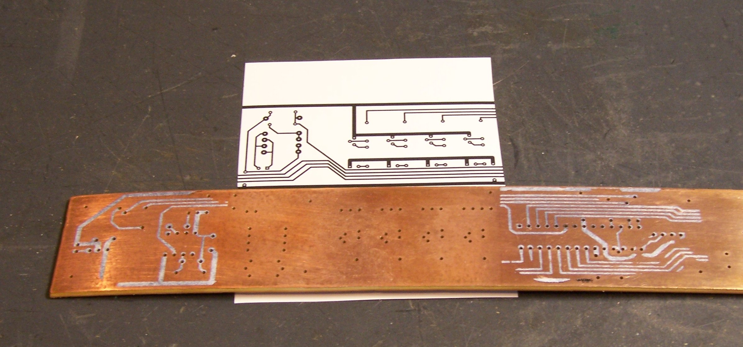
Because the 16.8″ length of my PCB was greater than the size of paper my printer accepts, and because the printer doesn’t seem to print at exactly accurate size, I used the GIMP to chop the image into three pieces, to iron on in sections. I split the image in areas with no holes and all horizontal traces so it’d be easy to line up, and I left about 1/4″ of overlap at each joint so I’d double up toner on the board rather than taking any chance of having a gap.

Ironing laser toner onto a PCB for etch resist, in sections

I ironed the two outer sections onto the board using our household iron set at 350°F and no steam, then soaked the board for half an hour to soften the paper and carefully peeled it off.

Iron-on PCB toner transfer with poor adhesion

A lot of the traces came off with the paper. It didn’t feel like I had peeled the traces off the PCB — it felt like they had never adhered in the first place. Reinforcing that suspicion was how much effort it took to clean the traces off the board and start over — the ones still on the board were well stuck. I ended up using acetone to clean them off the board.

I printed another copy and ironed it on, using the maximum temperature on the iron and the Giles Corey method (more weight). This time I soaked the board for over an hour. Once again, large sections of traces peeled away.

Press ‘n’ Peel Blue and Successful Ironing

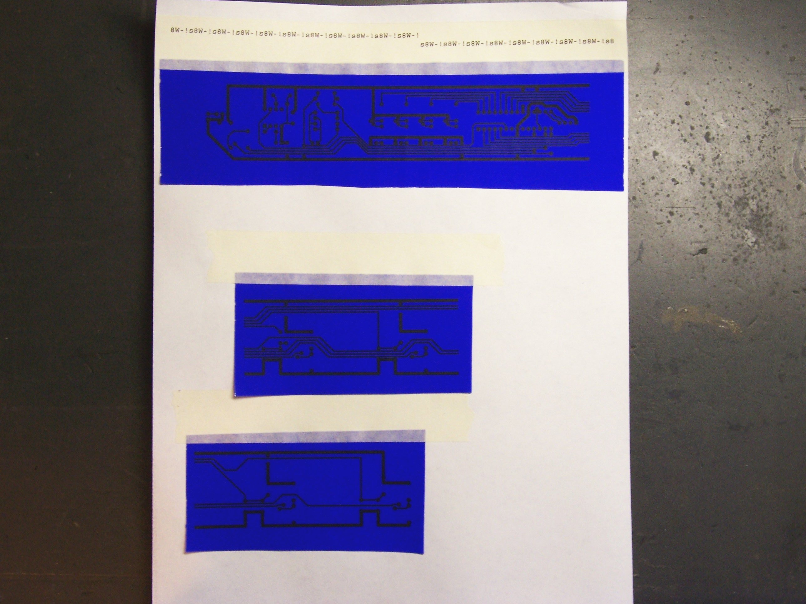
I have a few sheets of Press ‘n’ Peel Blue that Joel bought and encouraged me to test drive, and I’d had reasonably good luck the previous time I tried them, so I got them out. To avoid wasting an entire sheet of Blue, I printed the design onto a carrier sheet of plain paper, then cut appropriate-sized sections of Blue and masking-taped them to the paper over the printed areas and printed again.

Press 'n' Peel Blue

You can see across the top where my printer went nuts printing PostScript source code on the first try, but I got the design printed onto the Blue on the second try. I ironed a section of Blue onto the freshly-scrubbed PCB board, and . . .

Press 'n' Peel Blue iron-on PCB transfer; no adhesion around holes

Excellent adhesion most places; terrible adhesion around the holes.

So what’s different about the holes? I think they’re dimpled from when the drill hits the copper and before it starts to bite. The surface is slightly lower, and there’s not enough pressure to adhere the Blue (or the plain-paper transfer) to the copper.

I needed something between the iron and the transfer to help distribute the pressure, even down into slight surface variations. I considered a sheet of felt, but I was afraid that it would be too soft to distribute the pressure well. I settled on a kitchen paper towel folded in half, and voila!

Press 'n' Peel Blue iron-on PCB transfer; good adhesion throughout

Good adhesion everywhere!

Lesson: Use a thin pad between the iron and the toner transfer to help distribute pressure through surface irregularities.

Etching

I had struggled for a couple of weeks to think of an appropriate etching tank for a board of this size. I needed a plastic or glass tank long enough for the board — but preferably also narrow, so as not to require a huge amount of etchant to cover the board. Finally I thought of a section of PVC pipe, capped and slit in half. $20 and a trip to the bandsaw later, I had an etching tank. (Two, actually.)

Lesson: It’s surprisingly difficult to fully seat a cap on 3″ PVC before the cement sets.

PVC etching tank

I set the tank over the bathroom sink with the ends on paper towels, in case my PVC glue joints weren’t watertight. Good thing, too, since they weren’t. By the end of the etch, one of the paper towels was stained, and I was particularly glad I’d used it.

Lesson: Use lots and lots of PVC cement to get watertight joints for odd configurations and applications.

At first, the etchant appeared to be removing quite a bit of copper, as evidenced by its increasing opacity. Half an hour in, though, not much was happening, even though I dropped by every few minutes to agitate the tank.

After a while, I got the bright idea to heat the etchant with my heat gun, and the etching really took off at that point, proceeding at a nearly visible pace.

Lesson: Heat the etchant to at least 100°F.

Once all the unwanted copper was etched away, I used a plastic fork to remove the board from the tank and rinsed it under lots of running water. Then I went to the kitchen sink to filter the used etchant into an empty plastic bottle for later reuse.

Lesson: Coffee filters pass about 1/4 cup of liquid etchant before becoming strangely impermeable.

Lesson: Impermeable coffee filters do not make particularly good funnels.

Lesson: Poor funnels tend to spill liquid over the edge into the white porcelain sink.

Lesson: Poor funnels tend to slip down inside the plastic bottle.

Lesson: The nooks at each end of capped PVC hold quite a bit of etchant that spills all over when you’re trying to pour it out.

Lesson: Start the etchant recovery process a couple of hours before your wife comes home so you have plenty of time to scrub the sink.

Results

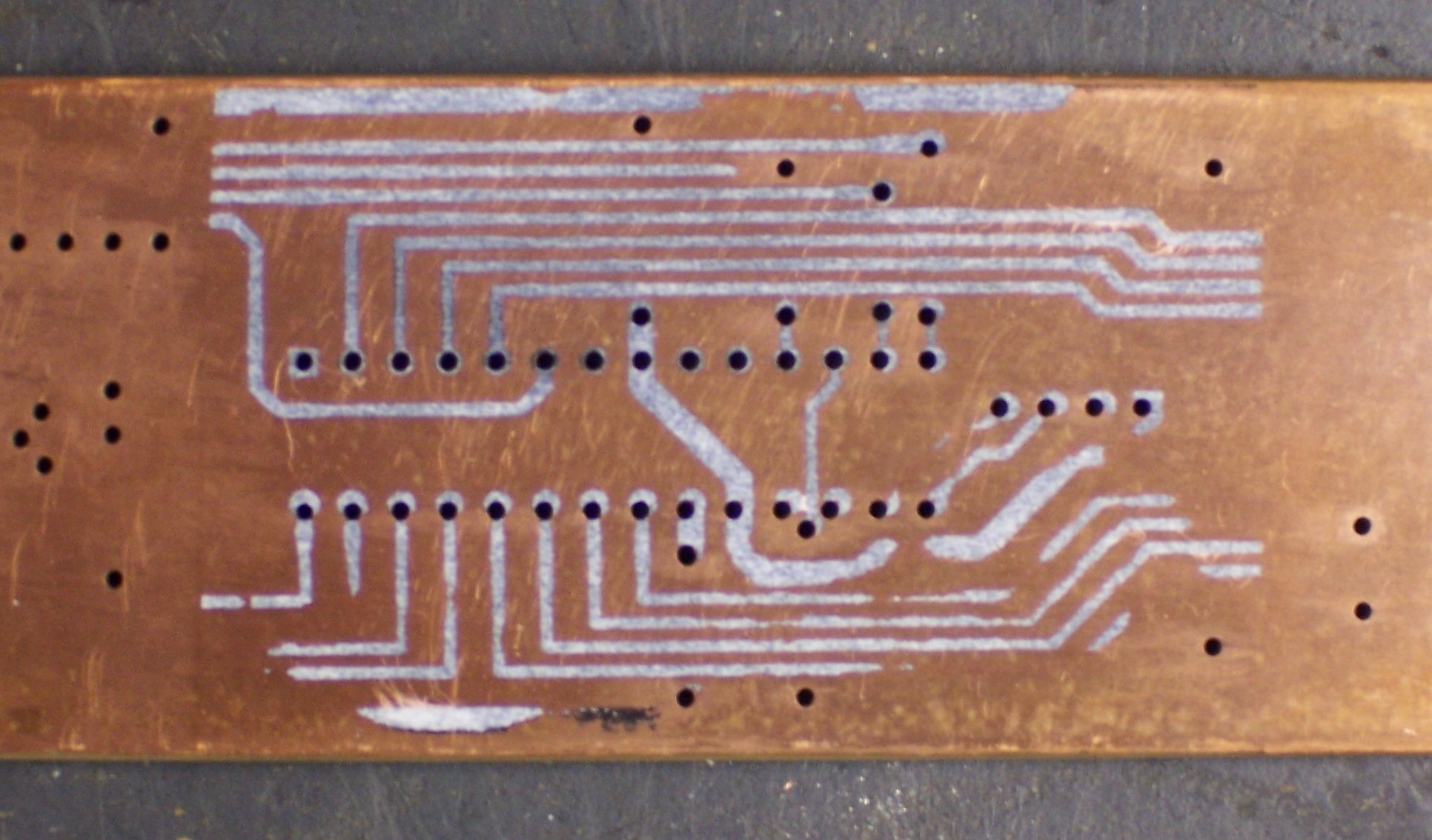
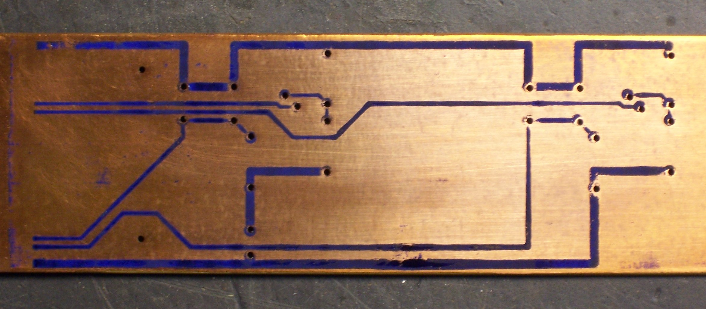
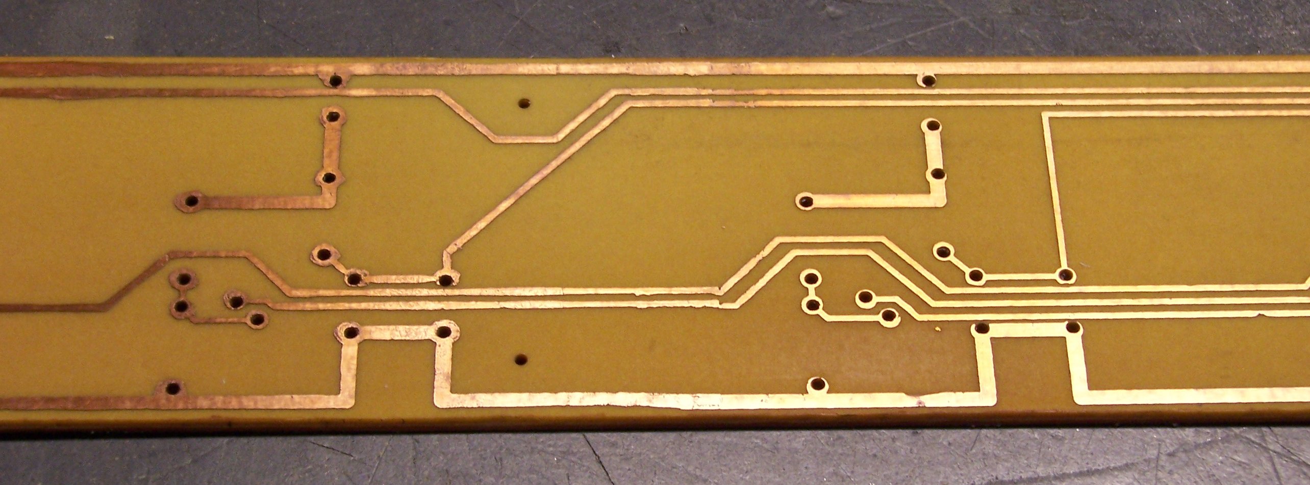
Etched, cleaned PCB

After cleaning the toner off the board with acetone, the traces really look nice. They have reasonably crisp edges and not too bad dropouts. This ended up being one of the nicer boards I’ve made by home etching.

Lesson: Try plain-paper toner transfer next time, using the paper towel pad trick.

PCB Layout and CNC Drilling Problems (and Solutions)

August 6th, 2007 by Keith Neufeld

I recently finished the prototype of my latest project (to be described in an upcoming post), and I made a lot of mistakes in PC board layout and construction. Like the SparkFun gallery of prototypes, I thought it was worth describing my problems and their solutions, to help myself and others avoid them in the future.

I’m doing that in two forms: a couple of detailed blog posts, and a new page with a summary version of the solutions. In the blog form, I’ll describe the problems in the order I encountered them; on the tips page, I’ll list the solutions in the order they’d be used when doing it right the first time.

Fitting the Case

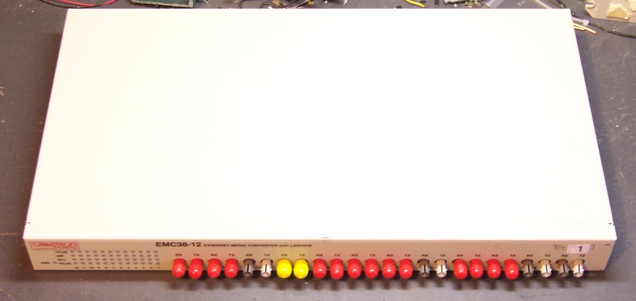
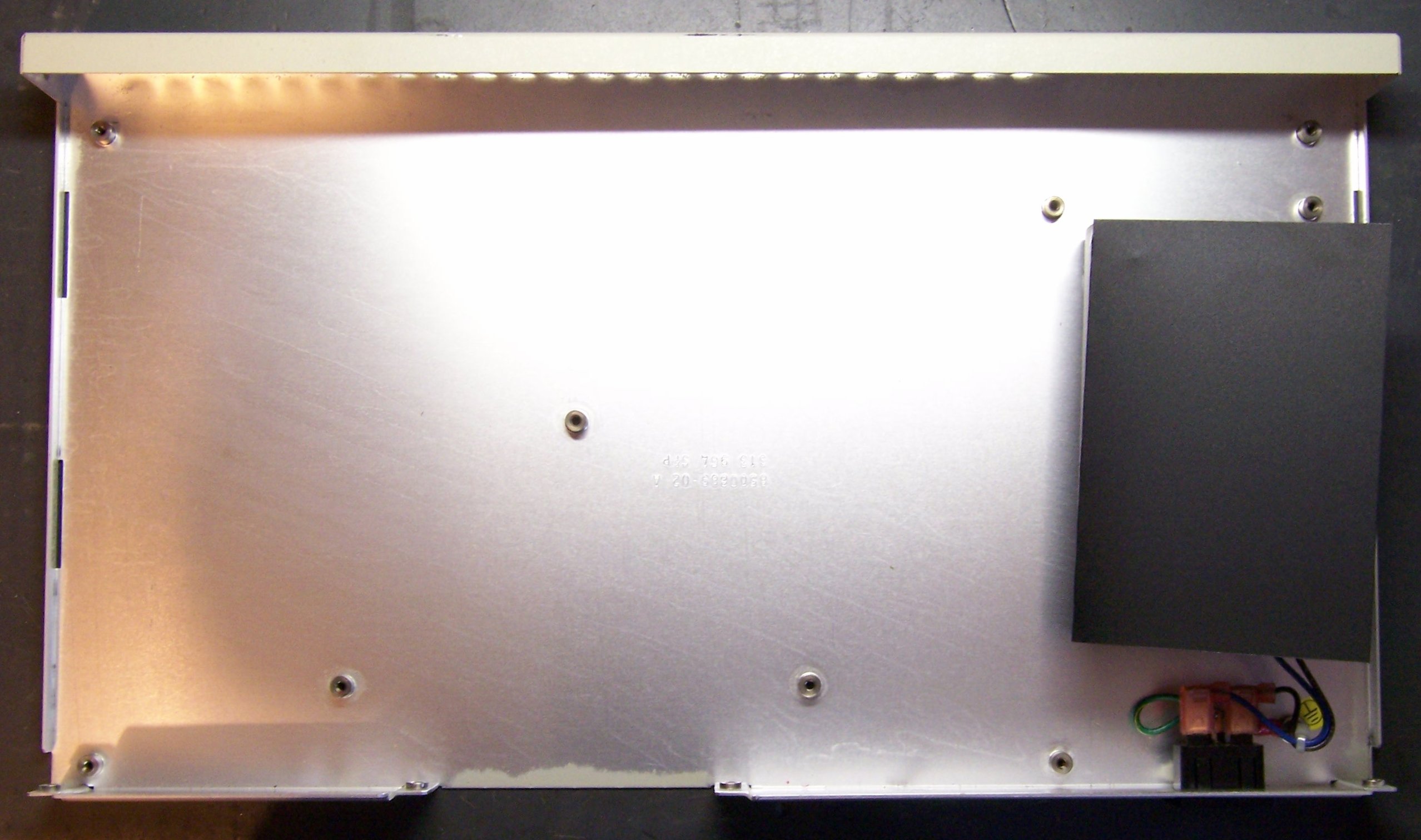
The project I’m building is a control device for my stereo system, so I wanted to build it in a rackmount case. Rackmount project boxes seem to be inordinately expensive ($40+); so for the prototype, I salvaged a piece of dead network equipment (rackmount 12-channel 10M fiber-to-copper media converter), ditched the guts, and kept the case. The power supply was on a separate board and turned out to be 5V, so I left it in place to drive my circuit.
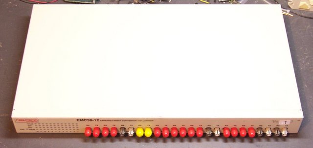
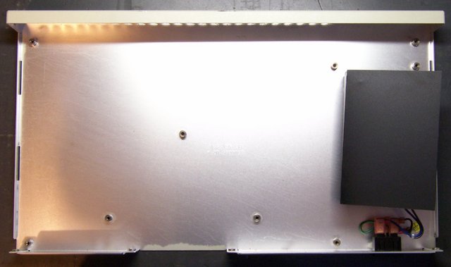
Rackmount fiber to copper media converter

Empty rackmount case with power supply

I needed pushbuttons and indicator LEDS on the front panel, so I planned my PCB to mount behind and parallel to the front of the enclosure. I measured the outside of the case and subtracted a generous .1″ from each edge to account for the thickness of the metal and to provide clearance around the edges of the PCB.

For the prototype, I decided to use the existing holes in the front panel for my LEDs and pushbuttons. I measured their approximate distances from the lower left corner and placed the components in the PCB layout program accordingly.

First mistake: When I measured for the size of the PCB, I didn’t look closely enough at the case. Where the top cover fits into the front edge of the case, there’s an extra lip underneath. I made the first board layout too tall to fit.

Lesson: Don’t make assumptions about the fit of the case. Inspect and measure where the PCB will actually fit.

Fortunately, before making a board, I printed the silkscreen layer and board outline from the layout software (FreePCB), cut and taped the pieces together, and held it inside the case to test the fit. I realized my error at that point, and correcting it was a (relatively) simple matter of changing the board outline and moving components and traces. I also tweaked the positions of the LEDs and pushbuttons for a better fit with the front-panel holes.

Auto Power Sequencer, top silk screen layer

Lesson: Print the board design on paper to test-fit into the enclosure before making a real board.

Challenges of a Single-Sided Board

I could have designed most of the circuitry using 7400-series digital logic, but some of the override functions I wanted to provide on the front panel would have got tricky, so I used a PIC microcontroller running the LogoChip language.

In order to perform firmware updates, I needed to include a serial port, but I didn’t really want to clutter the back panel with something that would be used so infrequently. For my own use, I like connecting with what I affectionately call a “Cisco blue cable,” the DB-9 to RJ-45 serial cable that ships with every piece of Cisco equipment (so I have a carton full of them). That meant putting an RJ-45 jack inside the case, and the problem was where to put the jack.
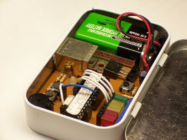
LogoChip in Altoids tin

Normally a jack would mount on the component side of the PC board, like the one up against the battery in my Curiously Strong LogoChip case, but here the component side was going to be pressed up against the inside of the front panel. Not only would that make the jack inaccessible (buried between the PCB and the front panel), but the jack was taller than the mounting hardware I wanted to use, and would have pushed the board too far back from the panel.

On a double-sided PC board, I could have mounted the jack on the “back” side and soldered it from the top. On my single-sided board, though, I’d have no way to solder it to the back-side traces — the jack itself would occupy the same space the soldering iron needed to.
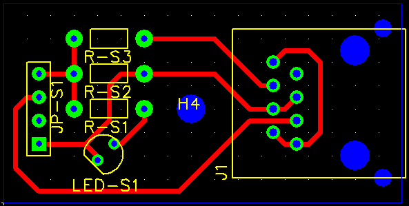
Auto Power Sequencer, serial board

I decided to settle for making a very small daughterboard, just big enough for the jack and supporting components, to mount to a spare post in the bottom of the case. I wasn’t wild about the idea, but at least it’d get me by. In fact, I ended up scrapping the serial board idea and hooking up a temporary jack, for reasons I’ll describe later.

Lesson: Plan ahead for bulky components.

Drill Bits

Once I (thought I) had the board design finalized, I generated an Excellon drill file to take to Joel’s house and drill on his CNC machine. Because his machine has only about 12″ of travel and I needed to drill a 16.8″ panel, I needed to split the holes into two sections, so I could rotate the board halfway through and resume drilling from the other end.

To do this, I picked a spot to divide the board where I had a relatively long run of traces with no holes nearby. That way, inevitable alignment problems could be corrected by slanting the traces from both sides to meet in the middle.

I wrote a set of scripts for selecting, rotating, translating, and mirroring hole data in Excellon drill files. (I’ll post these after I clean them up a bit.) I also wrote a script to remove Excellon tags that Joel’s DanCAM software doesn’t recognize. (I had earlier created a drill export specification to generate DanCAM from EAGLE, but I was using FreePCB due to the larger board size.) I wrote up a nice Makefile to control the whole process, so I could export new drill files and just run make to get the new copies for Joel’s machine.

I cut a strip off my giant PC board from Slim, cut a couple of sections to length, and went over to Joel’s to start drilling. I decided to drill the boards copper-side-up, so I’d have less tear-out to sand off afterward.
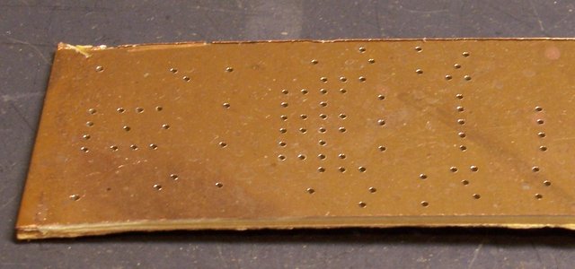
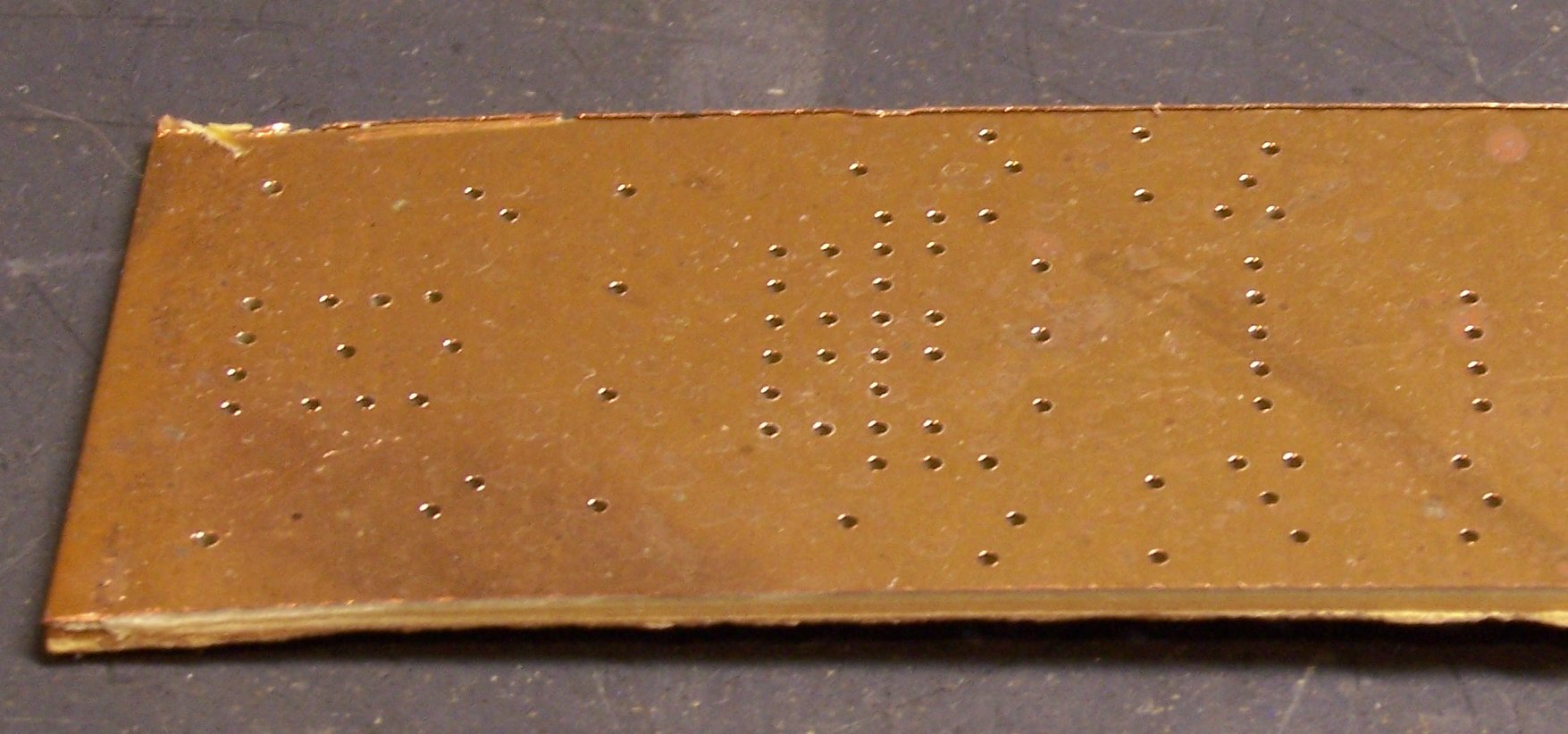
PCB board with drilled holes

Lesson: Drill with the copper side up. It leaves perfectly clean holes that don’t need sanding.

I drilled the first board, and half of the third board, as a top-to-bottom mirror image of the correct hole placement. I drove back and forth across town to get more boards way too many times.

Lesson: Check drill file mirroring very carefully, to make sure it matches the placement of the board on the drill table.

I also ended up breaking something like four bits, mainly due to operator error. In the CAM software, you enter the heights of the Z axis with the drill bit up (out of the board) and down (drilled into the board). At one point, I miskeyed the up position lower than the down position, causing the machine to move the table with the bit lowered into the board. Snap. I always do a dry run before letting it drill the whole board, but it had already dived into the table before I could abort.

The machine was also drilling fairly aggressively for the size of bit I was using, resulting in the breaking of another bit. I slowed it down and didn’t break any more after that (I think).

Lesson: Be aware of CNC machining parameters, particularly those relating to position and speed.

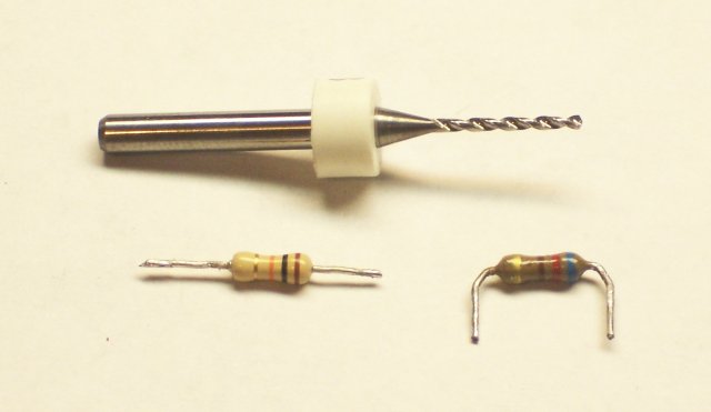
But I didn’t start out with very many small drill bits, and each time I broke the smallest remaining one, the holes I was drilling got larger and larger. By the time I got the board finished with all the holes in the right place, I was using a 39-mil drill bit, which was way larger than I wanted — way larger than my component leads.
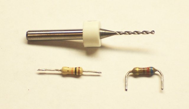
drill bit

Lesson: Stock up on appropriately-sized drill bits.

I’ve since placed an order with Drill Bit City for a couple of 25-packs of 5 each even sizes #72 – #64.

Drill Path

The hole list in the Excellon drill file isn’t in any particular physical order — the hole order probably has to do with the order the parts were imported into FreePCB from the partlist. DanCAM has an optimizing stage to reorder them into a more optimal path for the slow machine to travel, but I’ve noticed in the past that its idea of optimal seemed really strange and . . . suboptimal.

This time, I caught on to what was happening. DanCAM (at least the way we’re using it) doesn’t support changing drill bits to drill different-sized holes, so I drill all the holes with the same size bit. But internally, it’s still paying attention to the drill size, and optimizing each different bit’s path as a separate pass across the board, resulting in much unneeded movement when drilling with a single bit.

I updated my FreePCB Excellon to DanCAM conversion script to reduce the drill rack to a single size bit, and the next optimization and drilling operation went much faster than before — so much so that it felt like a qualitative rather than merely quantitative difference in drilling speed.

Lesson: If you’re drilling all the holes with the same size bit, make sure the machine knows that.

Having optimized the drill path so much better than before, I noticed that the machine was occasionally drilling the same hole more than once. I knew immediately why that was: Due to a quirk in the way FreePCB routes traces, there were numerous places on my board that I had multiple logical vias at the same physical location.

I wrote a very simple drill-uniq script to remove duplicate holes:

my %seen;

while (<>) {
    next if /^X/ && $seen{$_}++;

    print;
}

And the drilling operation got faster yet.

Lesson: Eliminate duplicate holes from the drill file, if the CNC machine isn’t smart enough to do it for you.

CNC Stepper Speed

My PC board production sequence is to drill the holes with the CNC machine, then print and iron on a toner transfer, then etch away the visible copper with ferric chloride. For the iron-on process to work, the predrilled holes need to align exactly with the printed copper trace pattern. I’ve noted in the past that they generally don’t align across the entire length or width of the board, and attributed that to inaccuracies in the paper feed rate of my laser printer.

This time, while I was waiting for one of several iterations of board to be drilled (due to my continuing errors), I checked the registration of the previous iteration and found it to be so bad that I got a ruler to find out exactly where the error was. It turns out that the answer was both — the drill and toner spacing were both wrong. Holding two iterations of drilled PCB up to the light revealed that the drill wasn’t even consistent from one pass to the next.

Since it’s a CNC drill, the only way that should be possible is if the steppers are skipping steps. If you push a stepper motor too fast, it skips (lags) a little bit, and stays out of sync until the next time you send it to the home position to check where it is. DanCAM’s setup process includes tests to make sure the motors are staying synchronized, but it’s pretty hard to tell if they’re losing only a few steps.

I went through the motor speed calibration section again, which boils down to running the motors faster and faster until they’re obviously losing steps, then backing off the speed until they seem stable again. I backed the speed off further than before, and on the next drill pass got all the holes as close to where they belonged as I was able to measure (except three that just randomly went a little bit off — still don’t know why, but I don’t think it was lost steps).

Lesson: Make sure the feed rates are within the steppers’ and drivers’ capacity.

At this point, I finally had a board that fit into my enclosure, with all the holes drilled (pretty much) where I wanted them. And a lot of things to remember to do better the next time.
Shhhhhh! (Quieter Fan for My Switch)

July 16th, 2007 by Keith Neufeld

The fan in the network switch in my home office is too loud. It’s the loudest thing in the whole room — louder than my newish and very quiet Dell PC. (Fedora, installed before ever booting the preinstalled XP Home, in case you wondered.)

I’d rather not have a switch there at all, but the DSL comes in on the ground floor (where my office is), I’ve tucked my server down in the basement, and I haven’t installed structured cabling yet. (The house is a hundred years old and the crawlspace is . . . interesting.) I need more connections going back and forth than I have cables, which means using a switch.

The Cisco switch I was using had only 100M ports, but my workstation and server both have integrated gig ethernet, so I was looking to upgrade the switch anyway.

I recently bought an old Linksys GigaSwitch EG0008 on eBay. It’s a 1U rack case with only eight gig ports on it — pretty much an antiquated beast. I was hoping it’d use passive cooling or at least have a quieter fan than my Cisco 1924.(*) Boy, was I wrong.

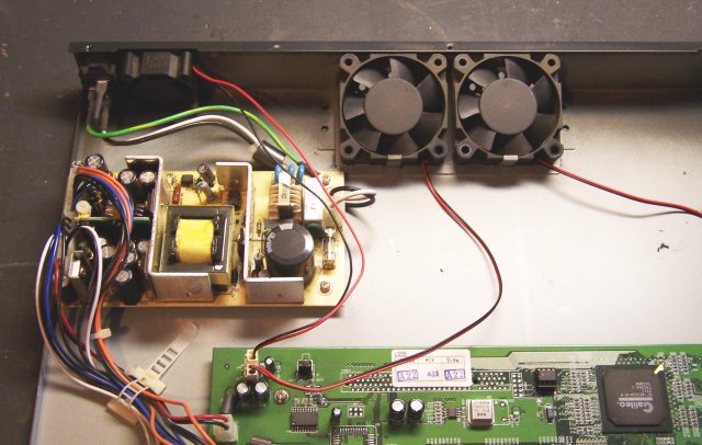
Cooling fans in Linksys EG0008

The Linksys has three fans, each loud. Two are in the center of the back, and there’s a separate one by the power supply. I took a little time yesterday to try to quiet it down.

Before

I used my sound level meter (an older version of this Radio Shack meter) to measure how loud each fan was. This was a very informal test intended just to give me a general idea; and due to the range of the meter, I measured from about 10cm away instead of the standard 1m.

I unplugged two fans at a time so I could test each fan individually. The small fan in the corner was the loudest, at about 58dB. Each of the two larger fans in the back registered about 57dB. With all of them running, I got about 62dB total.

Fan Changes

The first step was simply unplugging the two larger fans in the back. In an unventilated wiring closet, or stacked in a rack with other hot equipment, I’d want all the forced air I could get through this thing. But sitting in my office on a small stand under the base of my LCD monitor, it’s not going to get very warm. It probably doesn’t need any fans there, and one should certainly be enough.

With only the small fan plugged it, the volume dropped to slightly louder than my Cisco. Not good enough.

The small fan sounded a little rough to me, so I peeled back the sticker and added a drop of oil to its axle. It smoothed out a bit, but still not good enough.

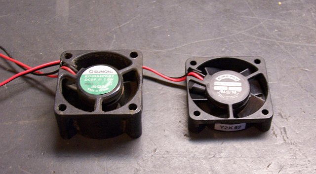
I had another 40mm fan on hand that I bought last year from All Electronics, so I soldered a connector onto it and hooked it up to the power. Sitting out in the open, I measured it around 54dB, so it seemed to be an improvement.

Original and replacement cooling fans from Linksys EG0008

The original fan wasn’t mounted with screws or bolts, but rather by snapping into position. With the replacement fan being so much slimmer, it no longer fit the slot. Since this isn’t for a ruggedized mobile application where things bounce around a lot, I just stuck it in place with hot glue.

Once in place, it measured about 58dB — the same as the original fan. Grrr.

Vent Holes

I noticed two differences in the sound of the replacement fan between when it was sitting in the open and when it was mounted in the case. The case acted as a sounding board to amplify the fan’s noise; and there was considerable wind noise when the fan was in position. I didn’t really have room to isolate the fan from the case with rubber strips, but I did tackle the wind noise.

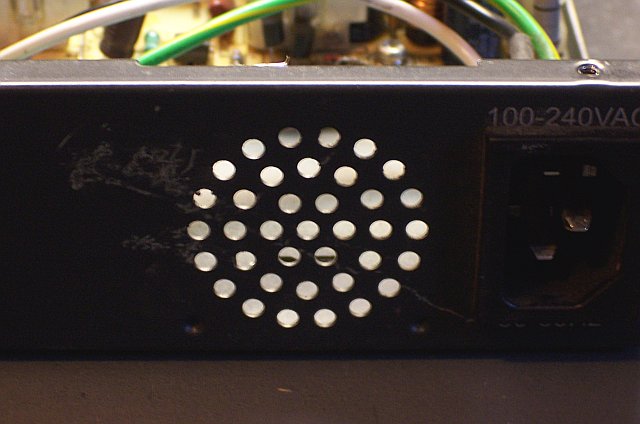
Original power supply vent holes in Linksys EG0008

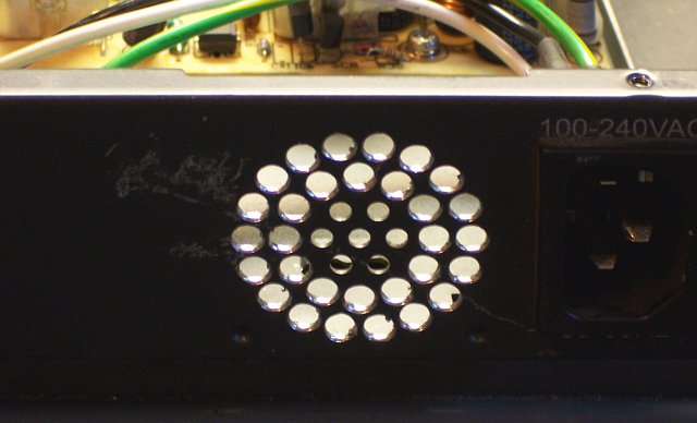
The ventilation holes behind the fan were not exactly what I’d call generously sized. I used my stepped drill bit to enlarge all of the holes that were in line with the fan’s blades.

Enlarged power supply vent holes in Linksys EG0008

After reinstalling the new fan, the overall noise level dropped to 54dB, a slight improvement over the first installation of the new fan and a considerable improvement over the original equipment.

I reassembled the switch and swapped it into service in my office, and it seems to be about as loud as the Cisco was. Interestingly, the pitch of the noise is a little different, so I notice it each time I step in the doorway. I’ll get used to it soon enough.

Closing Thoughts

In retrospect, since both the original and replacement 40mm fans measured about 58dB when mounted in the case before enlarging the vent holes, I could probably put the original fan back in and have approximately the same sound level improvement.

I’d like to find a quieter fan, though. I know there’s a whole market for PC case mods with really, really quiet fans. I’ll ask around and see whether anyone I know has a tested source. So rather than go back in to reinstall the original fan, I’ll hold out for a yet-quieter replacement.

Footnote

* Yes, I know the Cisco 1924 is a 10M switch. My 1924s have two 100M ports commonly used as uplinks; so at each end, one of the ports is the uplink and the other connects to the fast computer. The DSL firewall only gets a 10M port, which is faster than its WAN side anyway.

Current Project Prototype Almost Done

July 12th, 2007 by Keith Neufeld

FreePCB

Board layout is done, board is cut to size, drill files are converted to DanCAM format to drill at Joel’s house. I’ll print and iron on the etch resist after drilling. I’m going to try ironing on top-side “silk screen” like Cort’s been doing.

I drew the schematic in free EAGLE, but the board was too big to layout, so exported the netlist and imported to FreePCB. Substantially updated my eagle2pads netlist conversion utility, which I’ll be re-posting soon.

The FreePCB layout is so pretty, I just had to post it tonight.

Topics to cover after the board is made:

  • eagle2pads netlist conversion script updates
  • drill file selection and manipulation scripts and Makefile
  • custom etching tank
  • kits

Follow-Up to Driving a Bicolor LED from a Single Output Pin

July 1st, 2007 by Keith Neufeld

Within mere hours of posting yesterday’s entry about driving a bicolor LED from a single pin using the trick of turning the port into an input to make it tristate, “Mazzoo” posted an excellent comment, including this very insightful statement:

tristating or setting a controller pin as input, and leave it floating or (even worse) setting it to Vcc/2 is a reliable way to destroy the input gate.

That’s a very good point, and one that I hadn’t been thinking about (but hope I would have considered sooner or later).

Digital logic inputs depend on being high or low, and don’t deal well with inputs in the “dead band” in between. With many digital inputs, a voltage in the dead band puts the input transistors into their linear regions, which causes them to carry excessive current and overheat quickly. Deliberately putting digital inputs into the dead band for long periods of time would be a very bad idea.

Thus, to use this method for driving a bicolor LED, not only does the pin need to be changed to an input so it tristates, but it needs to be an A/D pin set to analog mode, so it doesn’t mind seeing a voltage in the dead band.

As I’ve described before, having a PIC pin set as an analog input changes the PORTX register from a read/write register to a write-only register, and you have to read the values from LATX, which messes up the LogoChip’s clearbit / setbit / testbit commands. But I’ll just have to work around that by using LATX instead of PORTX, because I can’t leave the pin floating in digital input mode.

Thanks, Mazzoo!

July 4:

It should also be safe to use tristating on a pin in digital input mode with a Schmitt trigger — pin A4 and all of port C. Unfortunately for me, the LogoChip’s design already uses most of port C, and I really wouldn’t have enough pins available to drive the four bicolor LEDs that I want to use in this project. So analog inputs it is.

Driving a Bicolor LED from a Single Output Pin

June 30th, 2007 by Keith Neufeld

I’m working on a control system for my stereo, with more information on that project to be posted soon. I was running into a problem having enough pins on my PIC to connect all the inputs, pushbuttons, LEDs, and outputs.

Yesterday I was talking to Tom and describing how each bicolor output LED requires two microcontroller pins to control both colors. I’m sure this scheme has been used a million times before, and I may even have seen it before, but I was very pleased to realize in a flash of insight how to drive a bicolor LED from a single output pin.

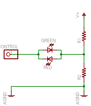
Driving a bicolor LED from a single microcontroller pin

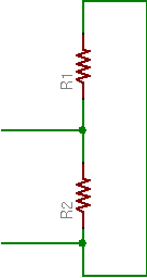
Instead of connecting the LED between the control pin and V+ or ground, connect it to a voltage divider between the two. Raise the control voltage to V+ and the green LED will conduct through R2. Lower the control voltage to 0V and the red LED will conduct through R1. Here’s the best part — change the control pin to an input and it’ll go into a tristate (high-impedance) mode, leaving the left end of the bicolor LED floating, with both elements off. Perfect! That saves my project!

I breadboarded this circuit with 330Ω resistors, and the LED was quite a bit dimmer than normal. Well, of course it was; it’s running off less voltage than usual. Plus the voltage divider isn’t exactly a stiff current source. But I was curious exactly how much less voltage (seems obvious, but wouldn’t it be nice to know for sure?), and what was the exact series resistance (ah, somewhat less obvious, eh?).

Thévenin Analysis

Thévenin’s Theorem states that any linear circuit (comprising only voltage sources and resistors) can be represented as a single voltage source and a single series resistor, and provides a very simple method to determine the equivalent voltage and resistance. So a Thévenin analysis of the voltage divider will give us a simpler model of that section of the circuit, which can then be used to determine the actual LED current.

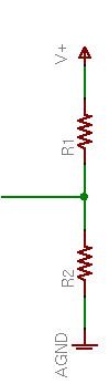
First, to determine the Thévenin voltage (VTH), mentally remove the load from the circuit and use Kirchhoff’s Law to find the voltage at the load connection.

Determining Thévenin equivalent voltage

In this case, assuming R1 = R2, VTH is V+ / 2.

Next, to determine the Thévenin resistance (RTH), (mentally) short out all the voltage sources and use Kirchhoff to find the overall resistance looking into the circuit.

Determining Thévenin equivalent resistance

In this case, mentally shorting V+ to ground puts R1 and R2 in parallel, giving

RTH = (R1 * R2) / (R1 + R2)

Or again in the case where R1 = R2,

RTH = R2 / 2R = R / 2

Thévenin Equivalent Circuit

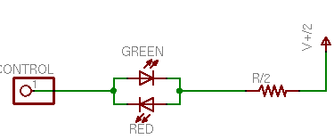
So assuming R1 = R2, the voltage divider is equivalent to a voltage source of V+ / 2 in series with a resistance of R / 2, which gives this simplified circuit:

Bicolor LED drive circuit with Thévenin equivalent voltage divider

This makes it easy to determine the LED current (ID). Whether the control voltage is at V+ or 0V, the LED and Thévenin resistor will see a voltage of V+ / 2 (forward or reverse).

Using the zeroeth approximation of a diode as a device that conducts electricity in a forward direction with no voltage drop, the resistor has the full voltage across it, so the resistor current

IR = (V+ / 2) / (R / 2) = V / R

and ID = IR. For a 5V supply and 330Ω resistors, I = 5V / 330Ω ≈ 15mA.

But that’s exactly the same current (and concomitant LED brightness) we’d expect running an LED from a full V+ with a full R, and I distinctly noted that the LED was dimmer. What’s going on?

LED Voltage Drop

The answer lies in the first approximation of an LED as a device that conducts electricity in the forward direction with a voltage drop and no resistance. The bicolor LED I was using has about a 2V drop in either direction (about 2.08V green and 1.95V red, at the temperature and moment I measured).

Still using a 5V supply and 330Ω resistors, an LED voltage drop VD = 2V gives a voltage across the resistor of

VR = (V / 2) – 2V = 2.5V – 2V = .5V
IR = VR / RTH = .5V / 165Ω ≈ 3mA
ID = IR3mA

Whoa! That’s a whole different story! Halving the effective supply voltage dramatically exaggerates the effect of the LED’s voltage drop.

In fact, to get back up to ID = 15mA:

RTH = VR / IR = .5V / 15mA &symp; 33Ω

That’s an order of magnitude lower current-limiting resistance to get the same LED current and brightness.

Even worse, note that this circuit (the original) has a continual current of V+ / 2R through the voltage divider. With 330Ω resistors, that’s 7.6mA (38mW), which may be tolerable in a non-battery-driven circuit; but with 33Ω resistors, that’s an unacceptable 76mA (380mW) per LED driver!

Tolerable Adaptations

So how can we make this circuit work well enough to be practical? Here are a couple of options.

First, note that the current-limiting resistance needed to be made so low because half the supply voltage is barely more than the diode’s voltage drop. With a higher supply voltage, more voltage would be “left” after taking out the LED’s drop, and a higher resistance could be used to get the same LED current.

But how far can we raise the supply voltage? For the circuit to work properly, the control voltage from the microcontroller needs to swing over the same range as the LED’s voltage divider. And alas, the PIC I’m using has a maximum VDD of 7.5V; or say a safe working voltage of 7V.

Adding 2V to V+ adds only 1V to the LED/resistor supply, increasing VR from .5V to 1.5V, or threefold. That translates into three times larger resistance and one third the voltage-divider power consumption — progress, but not as much as I’d like.

Second, note that the bicolor LED I’m using is not particularly high performance. Newer LEDs appear to me to be several orders of magnitude brighter at the same current. (Go check the amazing mCd claims of LED vendors on eBay. For the most part, they’re increasing efficiency, not current-handling capacity.) I’d gladly pay a little more for a much brighter LED that has lower current requirements for the same brightness.

Even one order of magnitude difference in LED efficiency pushes the voltage divider power consumption back into an acceptable level for the device I’m designing. It also cuts the power requirements for the PIC pin driving the LED. The datasheet quotes 25mA source or sink per pin, 200mA source or sink for all pins, but I’m old-fashioned and don’t want to push my luck.

One thing I don’t know is whether high-efficiency LEDs have the same voltage drop as traditional ones. With only 2.5V available for the LED, if higher efficiency comes at the expense of a higher voltage drop, I could “efficient” the circuit right out of its operating range.

Boosting the Drive Current

Before doing the actual calculations, I was pondering whether the PIC could really source and sink enough current to power all my LEDs as brightly as I want. I was musing out loud with Tom about how to build a transistor driver to buffer/boost the PIC’s output.

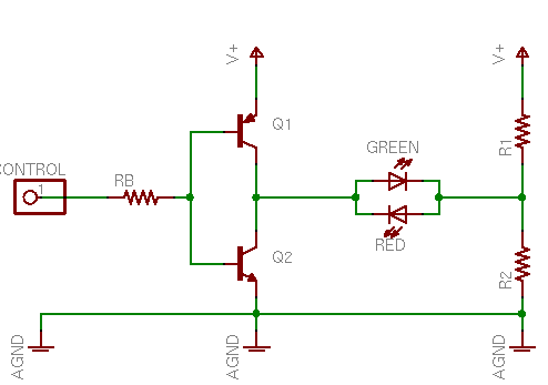
The driver needs to be a totem pole, meaning that it has two stacked elements so it can source the LED line up to V+ or sink it down to ground. The catch is the tristate trick that makes it possible to turn the bicolor LED off. Trying to cram a traditional complementary totem-pole output into this circuit IS WRONG AND DOESN’T WORK.

Bicolor LED circuit with incorrect totem-pole driver

When the control line is high, the upper (PNP) transistor is off and the lower (NPN) is on, so the NPN pulls the driver output low. Likewise, a low control line pulls the driver output high.

The problem is when the control line is tristated. Then current flows through the PNP’s emitter and base to the NPN’s base and emitter, turning both transistors on and shorting V+ to ground. Real totem-pole drivers are designed to make sure this can never happen, even during transitions.

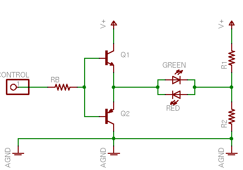
Here’s Tom’s solution, which like the tristate trick is probably a reinvention, but which is so clever that it still tickles me a day later to think about it.

Bicolor LED circuit with reversed totem-pole driver

Just swap the NPN and PNP transistors in the totem pole, putting the NPN on top and the PNP on the bottom. When the control line goes high, the upper (NPN) transistor is on and the lower (PNP) off, so the NPN pulls the driver output high. Likewise, a low control line pulls the driver output low.

And a tristated control line leaves both transistors off and the driver output in a high-impedance state, because the emitters aren’t connected to the power rails to conduct through the bases any more.

Brilliant! Makes me want to use it, even though I realize with high-efficiency LEDs I no longer have any technical reason to. :-) But I’ll keep it in my bag of tricks.

Green Lines in My LCD Projector

June 28th, 2007 by Keith Neufeld

I recently bought an ancient Sony “LCD Data Projector VPL-351Q” (video projector) on eBay for a reasonably modest price, without realizing just how ancient (and huge) it was. Fortunately, I was shopping geographically and was able to pick it up in person; it would have cost me a fortune to ship.

I’m interested in setting up a projector in the family room for watching movies, and this was a very affordable way to experiment before committing to an expensive course of action.

Sony LCD Data Projector VPL-351Q

That’s my 19″ stereo cabinet this thing is sitting on, with candlesticks elevating the front feet. It’s immense.

Old Lamp (Bulb)

Each time I power up the projector, it tells me that its lamp is old and needs to be replaced soon, which is no great surprise. (The onset of a lamp replacement warning seems to be a pretty strong motivator to retire projectors that are getting old anyway.) Of course, the few vendors I can find selling replacement lamps want $500 and up for them — a healthy order of magnitude more than I paid for the projector. Ha ha. This lamp is a bit dim, but not $500 dim.

I’m very curious how the projector knows the lamp is old — by counting hours of use (with a timer that I could reset?), or by monitoring lamp current. I’m also intrigued by the idea of rebuilding the lamp using something else — an automotive halogen bulb, perhaps. I assume I’d need to reuse the same reflector, and I think I might be able to manage it.

I’d also have to rig a different power supply for the replacement bulb — the original appears to run on 70V. The real problem would be if the projector monitors the bulb voltage or current (that I was no longer using) and shuts down if it seems improper. I’m not sure I’d be willing to go to the effort to rework or disable such a circuit.

Green Lines

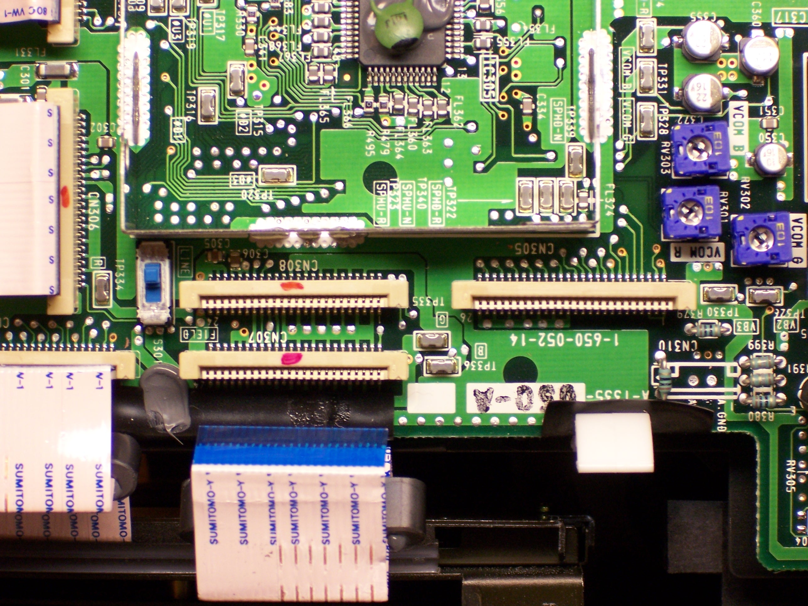
Worse than the brightness, though, is a pair of green lines across the screen, just below the middle of the display. When I got it home and discovered them, I popped the case to have a look and found that the projector has a beam splitter, three monochrome LCD screens with color gels, and a beam . . . uh . . . unsplitter. So it’s plausible that the problem is isolated to the green LCD, and perhaps is nothing more than something is wrong with a row control line.

Image from my video projector with green lines

The black line, BTW, is a halogen torchiere — I’m temporarily projecting this onto the wall behind the couch. We’ll rearrange the furniture if it works out.

Inside the case, each LCD has two flex-PCB cables, presumably for row and column select. If the silk-screened labels are to be believed, the connectors in the upper center and right of the picture control the blue LCD, the lower center and left control green, and the one on the left plus the one disappearing off the upper left control red.

Sony VPL-351Q LCD control PCB

LCDs with which I’m familiar are clear when idle, and opaque when active. (Think of an LCD calculator or monochrome PDA — they’re grey when they’re off, not black.) If that’s how these LCDs work, then the bright green lines are rows that are letting green light through all the time — rows that are transparent all the time — rows that are never getting activated. Maybe I just had a bad connection on a pin or two.

(The connectors don’t have nearly as many pins as the horizontal and vertical resolution of the LCD, so my hypothesis isn’t perfect. A one-to-one match between control lines and rows would make a pretty compelling case. But even with row multiplexing or addressing, a single address line could still impact only one or two lines. Mmmmm . . . okay, not really; at least not two that close together. But bear with me.)

So the first thing I did was pull the cables for the green LCD, clean their contacts, and reassemble. Alas, no change.

Cold Solder?

Still chasing the notion of a bad connection, I wondered whether one of the ribbon sockets might have a bad solder joint. Logically it should be the green row controller; and since the LCD has lower vertical resolution than horizontal, that means it should be the smaller of the two green connectors — the one in the lower left.

Tonight I put the SMT tip on my soldering iron and went to reheat the solder job on the green connectors — on both green connectors, for good measure. I did reheat them — I made some nice solder bridges, and I think lifted a trace or two. When I tested the projector again, I had every seventh blue column missing (I had absent-mindedly touched up the wider blue connector also — so wide == columns), and some other strange artifacts.

Not yet deterred, I reheated the solder joints again. This time, though, I used the heat gun to do a more consistent job. I was concerned that the sockets were plastic and would melt before the solder reflowed; but I kept a close eye on them, and although they got a bit darker, they didn’t melt a bit. I knew I got the solder to reflow because the SMT slide switch actually tipped over sideways from the airflow at one point, then popped itself back up when I backed away.

The heat gun was the right approach and surface tension is my friend, because that treatment fixed the ills I had just caused. The projector is now back to two horizontal green lines.

What Next?

I’m curious how the ribbon cables attach to the LCDs. It still seems plausible that I have a bad connection somewhere, and perhaps that bad connection is at the green LCD itself. LCD elements that I’ve played with don’t have wire connections — everything on the glass is next to invisible, as if it’s painted on with disappearing ink. Connections are made by pressing metal or anisotropic rubber contacts against the traces on the glass — maybe one of those connections needs cleaning?

I’m willing to dig in and examine the LCDs, but I’m leery of unmounting them. They’re obviously positioned very precisely to get the three screens’ pixels to align on the output, and I haven’t looked closely enough yet to see how that alignment is done. I’ll want to be sure that I can get the screens realigned properly before I consider unmounting one to examine its connectors.

If the problem isn’t the green screen itself, then likely a driver chip is bad, or has a bad connection. I’ll get there eventually.

Rebuilding a PowerBook G4 Battery

June 24th, 2007 by Keith Neufeld

I do all of my mobile computing — and my blogging slouched on the couch in my family room — using a hand-me-down 500MHz PowerBook G4. It was given to me used, battered, and obsolete two and half years ago, and after upgrading the RAM to 1G, installing OS X Tiger from a family license, and installing an AirPort card, it has served me well.

It’s starting to feel a little slow when loading bloated web pages, but my main complaint at this point is its battery life. I was given two batteries with it, one of which never held a charge at all. The second battery’s usable lifespan has slowly decreased from about three hours to around one, even when I turn off power to the AirPort card.

Worse, the battery meter still shows upwards of 60% charge remaining when it suddenly powers off with no warning. I’ve run Apple’s battery recalibration procedure several times, but it doesn’t make any difference.

Replacement batteries seem to run upwards of $80, and it’s impossible to tell from the online sales pages whether they’re original stock every bit as old as my own failing battery. I’m not afraid to dig into things and I’ve rebuilt my original Roomba’s battery before, so I decided to tackle this one myself. And since I had a spare battery that was already worthless, I could rebuild the spare without risking damage to my main battery that still mostly worked.

But it turned out I couldn’t find replacement cells at my usual surplus sites — they’re a little larger than AA, which was all I could find. eBay to the rescue. One of my favorite sellers is a surplus recycling center in Topeka. I get up to Lawrence enough that I buy a trickle of stuff from them, then pick it up when I’m in the neighborhood anyway, and save a bunch of money not having to have things shipped.

I started watching their auctions for notebook batteries. Not PowerBook batteries — but other batteries at low enough prices that I could cannibalize them for cells. Within a matter of days, I had purchased a Compaq and a Dell battery for $5 each. I’m well aware that they’re not likely to be brand new, but for only $5, it’s still worth trying them for a rebuild.

Today I got around to doing it.

Inside the Batteries

Here’s my original battery with the two donors:

PowerBook battery with two donors

And the same batteries with the cases removed:

PowerBook battery with two donors, tops removed

You can see that the Dell battery has only six cells, which aren’t enough to rebuild the PowerBook. They’re still available as donors; but as the Compaq has eight cells, the Dell’s won’t be needed.

The first step was making a careful diagram of the inside of the original battery, noting cell polarity and wiring connections. Here’s the top view:

PowerBook battery, inside view

And the resulting diagram:

PowerBook battery hookup diagram, top side

The heavy black lines along the tops and bottoms of the cells are foil strips spot-welded to the cells, joining them together two-by-two in parallel, and the pairs into a series string. When I took apart the donor batteries, I looked for sets of cells welded together the same way, to minimize unnecessary soldering during reassembly.

The bottom side had only two wires:

PowerBook battery cells, underside

So its diagram was trivial:

PowerBook battery hookup diagram, bottom side

Happily, the cells in the Compaq donor were spot-welded together in parallel pairs like the PowerBook cells, making reuse easy.

Compaq donor battery, end view

This set of four can replace either the left and middle or middle and right cells.

Notebook battery cells and alignment clip

Where a pair of batteries was spot-welded in parallel, both ends were connected rigidly and the two cells formed a solid assembly. But where only one end was connected in series to the next pair, the strip at that end acted as a hinge and the two pairs tended to flop out of alignment. The Compaq battery had clever clips sandwiched between parallel pairs to maintain alignment. At first I thought I’d be able to reuse the clips, but my PowerBook battery case had ridges sticking up between pairs, so I had to remove the clips.

Reassembly

After comparing the various spot-welded tabs on the new cells to those on the old, I decided which cells to put where and test-fitted everything into the case.

Rebuilding PowerBook battery, new cells fitted in place

Looks good! Now I needed to rewire.

The original battery had fine wires from the battery-control PC boards to the different cells, but also a few heavier-gauge wires directly from cell to cell. Rather than desolder those wires from the original and move them to the new battery, I looked around for similar-gauge wire. The motherboard wiring harness from a dead PC power supply looked perfect — and it’s even a little heavier gauge (20 instead of 22).

PC power supply motherboard cable harness

First I fitted and soldered the black and white wires on the underside that connect the upper and lower single cells into a parallel pair. I also made the series connection from their right terminal to the upper terminal of the right pair.

Next, I needed to connect the left pair in series with the center pair. The original battery had their upper terminals all spot-welded to the same strip, but the donor battery had a different cell configuration, so I needed to make that connection with wire. I chose yellow to match the yellow PCB fly wire that connects to the same junction. Now the inter-cell wiring was complete.

Rebuilding PowerBook battery, inter-cell wiring complete

Reconnecting the PCBs

I pushed the PC boards approximately back into place and started reconnecting their wires. Leaving for last the upper left connection with heatshrink covering some inline mystery component, I started on the bottom set of wires. I hooked up the small black wire from the lower left PCB to the lower left battery terminal, then the orange wire to the center of the lower side of the center cells.

As I soldered the brown wire to the right end of the lower cells, I smelled something funny — and it didn’t smell just like melted insulation. I quickly desoldered it and sniffed around. Convincing myself that it was just the insulation, I resoldered it.

Rebuilt PowerBook battery, mostly rewired

Then I noticed that the right two cells in the main row were warm — quite warm — and it had been a long time since I had soldered them. I desoldered every connection as fast as I could and sat back to think about what was happening. At that point, my infrared thermometer said that the rightmost cell was 100°F.

Connection Sequence Matters

There were only two good explanations: Either I had made an error in my rewiring, or it mattered in what order the cells were reconnected. After re-rechecking my connections, I redrew my diagram of the original battery to consider exactly how the cells were wired.

PowerBook battery polarity diagram

After seeing the diagram drawn out like this, it made sense to think that the order of attaching connections could matter. The black wire hidden in the lower left is the ground, and the red wire going to the connection I’d been saving for last is the positive output. The orange, brown, and yellow wires tap into the series chain between cell pairs, presumably to measure the health of each pair.

So . . . maybe the monitoring circuit didn’t like having the lower cells reconnected without the main V+ connected yet. By then, all the cells were back down to room temperature, and I cautiously reassembled them in the case. This time I made the red connection first, then the black, completing the overall circuit.

I checked the temperature of the cells again and it didn’t seem to be rising, so I reconnected the orange, brown, and yellow wires. After waiting a few minutes and checking the temperature yet again, I put insulating tape back over several of the connections and called it good.

Rebuilt PowerBook battery

Testing and Results

The battery case press-fits together well enough that it doesn’t need much help to stay closed, but I put a couple of pieces of clear tape on opposite sides to keep it from surprising me. If the rebuilt battery works well and seems worth using, I’ll probably replace them with thin, metallic foil tape.
I shut down my PowerBook and took it to the kitchen sink, where a hypothetical fire would be the easiest to contain with the least damage to the house. I cautiously put the rebuilt battery into the computer, and nothing blew up or got warm. I connected the power cable and its LEDs went orange, indicating that it was charging the battery. The battery’s lowest light flickered, also indicating a charge. So far, so good.

I booted OS X and watched the battery monitor on the menu bar. By the time the computer was up, the indicator showed 6% charge, climbing very quickly to 8% as I watched. Switching to time-remaining mode indicated 0:18 to a full charge. Hm, that doesn’t seem nearly long enough.

Well, after a few weeks of disuse, NiMH batteries often need several charge cycles before regaining their full capacity; maybe Li-Ion batteries are similar. I’ll run a few charge cycles and see.

The Trouble with the Old Battery

Out of curiosity, I put the meter across each cell pair in the old battery and measured the voltage.

Cell Pair> Voltage
left 2.09V
center 3.17V
right 3.20V
upper/lower 3.10V

It looks like just one cell pair — or maybe just one cell within that pair — was bad. Maybe the rest of the battery could reasonably have been salvaged — maybe I should still go back and replace just those two cells. If they were NiCd, I’d consider zapping them to burn out the fuzz crystals on the electrodes, but I don’t know enough about Li-Ion to know whether that’s safe (or useful) to do.

I’ll see how the rebuilt battery works before thinking too hard about this. Even if the cells I just installed aren’t the best, I’m guessing I could look around and get newer cells that’d be fresher and hold more of a charge than the better of the original cells, so it’s probably not worth trying to salvage the rest of the original battery.